NB3H60113GH3 Description
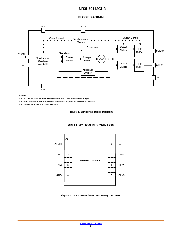
Pin Connections (Top View) WDFN8 .onsemi. Active Low Master Reset to disable the device and set outputs Low. Internal pull−down resistor.
NB3H60113GH3 Key Features
- Member of the OmniClock Family of Programmable Clock
- Operating Power Supply: 2.5 V ± 10%
- I/O Standards
- Input: LVCMOS Clock
- Output: LVDS
- 1 Programmable Differential Clock Output of 125 MHz
- Input Frequency Range
- Reference Clock: 25 MHz
- Power Saving mode through Power Down Pin
- Programming and Evaluation Kit for Field Programming and Quick