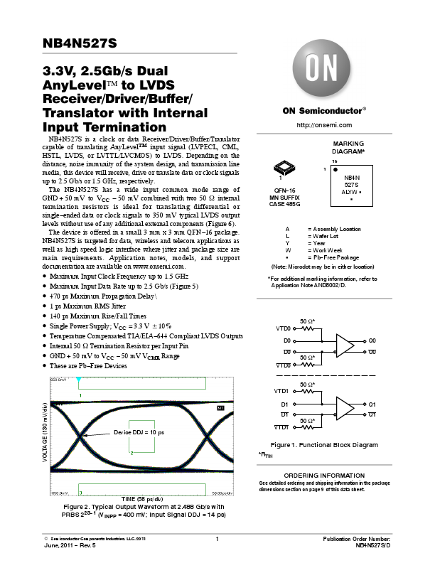
NB4N527S Description
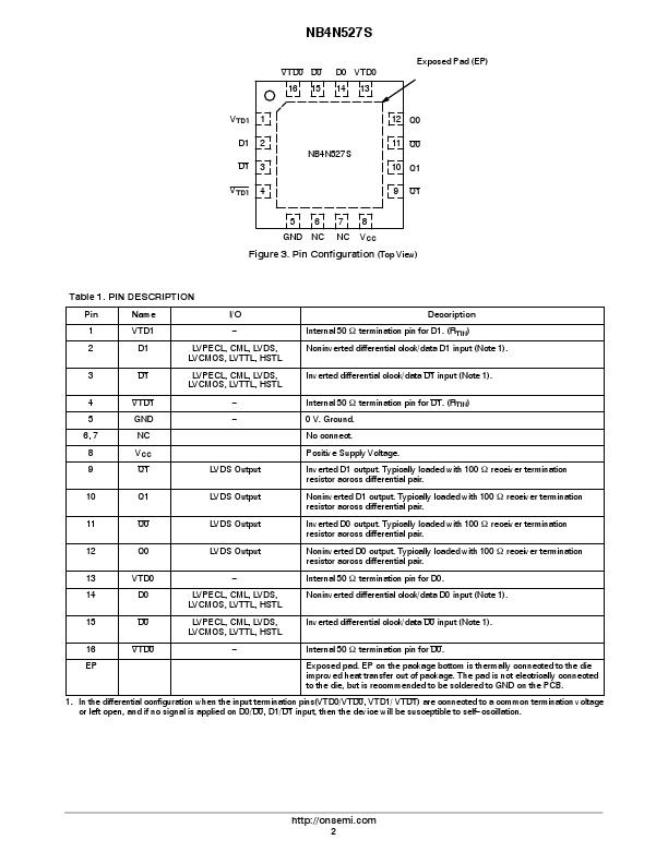
Pin Name I/O Description 1 VTD1 − Internal 50 W termination pin for D1. (RTIN) 2 D1 LVPECL, CML, LVDS, Noninverted differential clock/data D1 input (Note 1). LVCMOS, LVTTL, HSTL 3 D1 LVPECL, CML, LVDS, Inverted differential clock/data D1 input (Note 1).