P3P622S01J Description
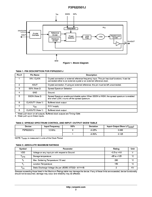
P3P622S01J is a versatile, 3.3 V Zero−delay buffer designed to distribute low frequency Timing−Safe Clocks with Peak EMI Reduction. P3P622S01J accepts an input clock either from a fundamental Crystal or from an external reference clock. P3P622S01J accepts one reference input and drives out two low−skew clocks.
P3P622S01J Key Features
- Low Frequency Clock Distribution with Timing-Safe Peak EMI
- Input Frequency Range: 4 MHz
- 20 MHz
- Zero Input
- Output Propagation Delay
- Low-skew Outputs
- Output-output Skew Less than 250 pS
- Device-device Skew Less than 700 pS
- Less than 200 pS Cycle-to-cycle Jitter
- Available in 8 Pin, 4.4 mm TSSOP Package