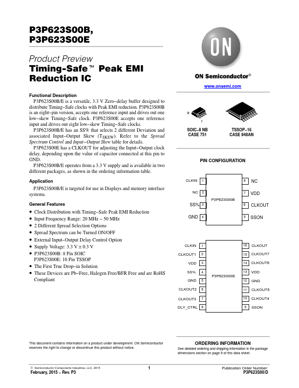
The following content is an automatically extracted verbatim text
from the original manufacturer datasheet and is provided for reference purposes only.
View original datasheet text
P3P623S00B, P3P623S00E
Product Preview Timing-Safet Peak EMI Reduction IC
Functional Description P3P623S00B/E is a versatile, 3.3 V Zero−delay buffer designed to
distribute Timing−Safe clocks with Peak EMI reduction. P3P623S00B is an eight−pin version, accepts one reference input and drives out one low−skew Timing−Safe clock. P3P623S00E accepts one reference input and drives out eight low−skew Timing−Safe clocks.
P3P623S00B/E has an SS% that selects 2 different Deviation and associated Input−Output Skew (TSKEW). Refer to the Spread Spectrum Control and Input−Output Skew table for details.
P3P623S00E has a CLKOUT for adjusting the Input−Output clock delay, depending upon the value of capacitor connected at this pin to GND.
P3P623S00B/E operates from a 3.