Datasheet4U Logo Datasheet4U.com

P3P623S09B - Timing-Safe Peak EMI Reduction IC

Download the P3P623S09B datasheet PDF. This datasheet also covers the P3P623S05A variant, as both devices belong to the same timing-safe peak emi reduction ic family and are provided as variant models within a single manufacturer datasheet.

General Description

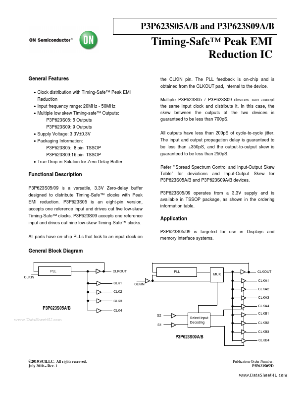
P3P623S05/09 is a versatile, 3.3V Zero-delay buffer designed to distribute Timing-Safe™ clocks with Peak EMI reduction.

P3P623S05 is an eight-pin version, accepts one reference input and drives out five low-skew Timing-Safe™ clocks.

Key Features

  • Clock distribution with Timing-Safe™ Peak EMI Reduction.
  • Input frequency range: 20MHz - 50MHz.
  • Multiple low skew Timing-safe™ Outputs: P3P623S05: 5 Outputs P3P623S09: 9 Outputs.
  • Supply Voltage: 3.3V±0.3V.
  • Packaging Information: P3P623S05: 8 pin TSSOP P3P623S09:16 pin TSSOP.
  • True Drop-in Solution for Zero Delay Buffer All outputs have less than 200pS of cycle-to-cycle jitter. The input and output propagation delay is guaranteed to be less tha.

📥 Download Datasheet

Note: The manufacturer provides a single datasheet file (P3P623S05A_ONSemiconductor.pdf) that lists specifications for multiple related part numbers.

Datasheet Details

Part number P3P623S09B
Manufacturer onsemi
File Size 224.24 KB
Description Timing-Safe Peak EMI Reduction IC
Datasheet download datasheet P3P623S09B Datasheet

Full PDF Text Transcription (Reference)

The following content is an automatically extracted verbatim text from the original manufacturer datasheet and is provided for reference purposes only.

View original datasheet text
P3P623S05A/B and P3P623S09A/B Timing-Safe™ Peak EMI Reduction IC General Features • Clock distribution with Timing-Safe™ Peak EMI Reduction • Input frequency range: 20MHz - 50MHz • Multiple low skew Timing-safe™ Outputs: P3P623S05: 5 Outputs P3P623S09: 9 Outputs • Supply Voltage: 3.3V±0.3V • Packaging Information: P3P623S05: 8 pin TSSOP P3P623S09:16 pin TSSOP • True Drop-in Solution for Zero Delay Buffer All outputs have less than 200pS of cycle-to-cycle jitter. The input and output propagation delay is guaranteed to be less than ±350pS, and the output-to-output skew is guaranteed to be less than 250pS. Refer “Spread Spectrum Control and Input-Output Skew Table” for deviations and Input-Output Skew for P3P623S05A/B and P3P623S09A/B devices. P3P623S05/09 operates from a 3.