AN8018SA Overview
Key Specifications
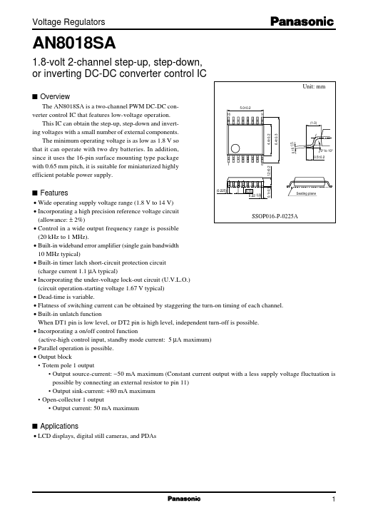
Package: LSSOP
Max Operating Temp: 85 °C
Min Operating Temp: -30 °C
Key Features
- Wide operating supply voltage range (1.8 V to 14 V)
- Incorporating a high precision reference voltage circuit SSOP016-P-0225A (allowance: ± 2%)
- Control in a wide output frequency range is possible (20 kHz to 1 MHz)
- Built-in wideband error amplifier (single gain bandwidth 10 MHz typical)
- Built-in timer latch short-circuit protection circuit (charge current 1.1 µA typical)