MN3880S Overview
Key Features
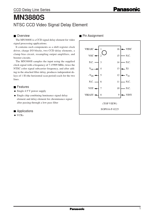
- VBB N.C. VOY VBIASY VINY N.C. N.C. VSS XI N.C. N.C. VINC Pin Name Output gate connection (C) Signal output (C) No connection Power supply Substrate connection No connection Signal output (Y) Output gate connection (Y) Signal output (Y) No connection No connection GND Clock input No connection No connection Signal output (C)