MN3885S
Overview
The MN3885S is a CCD signal delay element for video signal processing applications. It contains such ponents as a shift register clock driver, charge I/O blocks, two CCD delay elements, a clamp bias circuit, resampling output amplifiers, and booster circuits. The MN3885S samples the input using the supplied clock signal with a frequency 7.15909 MHz of twice the NTSC color signal subcarrier frequency, and after adding in the attached filter delay, produces independent delays of 1 H (the horizontal scan period) each for the two lines.
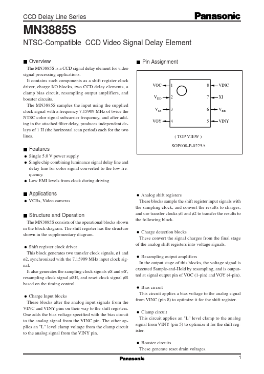
Pin Assignment
VOC VDD VSS VOY
1 2 3 4
8 7 6 5
VINC XI VBB VINY
( TOP VIEW ) SOP008-P-0225A
Features
Single 5.0 V power supply Single chip bining luminance signal delay line and delay line for color signal converted to the low frequency. Low EMI levels from clock during driving
Applications
VCRs, Video cameras
Structure and Operation
The MN3885S consists of the operational blocks shown in the block diagram. The shift register has the...