MN6153UC
Overview
The MN6153UC is a CMOS LSI for a phase-locked loop (PLL) frequency synthesizer with serial data input. It consists of a two-coefficient prescaler, variable frequency divider, phase parator, and charge pump. It offers high-speed operation on a low power supply voltage (1.0 to 1.4 V) and low power consumption (0.5 m W for VDD=1.03 V, F IN= 60 MHz). Other features include intermittent operation by the power save (PS) control signal and high-speed pull-in that rapidly corrects the phase differences occurring at the start of operation.
Pin Assignment
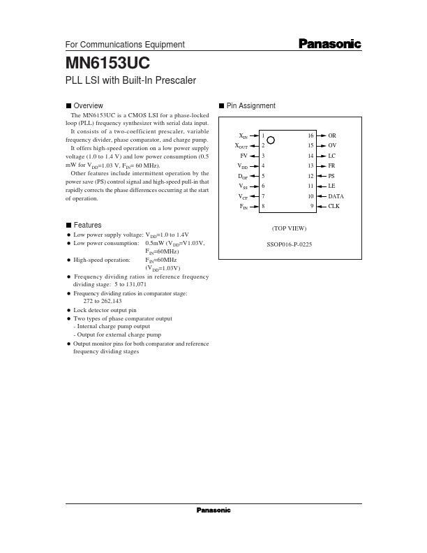
XIN XOUT FV VDD DOP VSS VCP FIN
1 2 3 4 5 6 7 8
16 15 14 13 12 11 10 9
OR OV LC FR PS LE DATA CLK
Features
Low power supply voltage: V DD=1.0 to 1.4V Low power consumption: 0.5m W (V DD=V1.03V, F IN=60MHz) High-speed operation: F IN=60MHz (V DD=1.03V) Frequency dividing ratios in reference frequency dividing stage: 5 to 131,071 Frequency dividing ratios in parator stage: 272 to 262,143 Lock detector output pin Two types of phase...