Philips 74LVC125
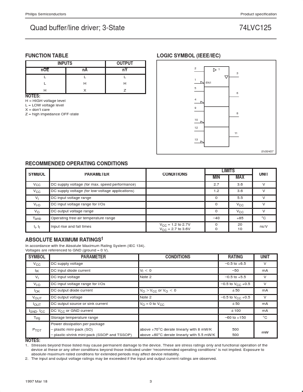
The 74LVC125 is a high performance, low-power, low-voltage Si-gate CMOS device and superior to most advanced CMOS compatible TTL families. The 74LVC125 consists of four non-inverting buffers/line drivers with 3-State outputs. The 3-State outputs (nY) are controlled by the output enable input (nOE).| Part No. | 74LVC125 |
|---|---|
| Datasheet | 74LVC125 Download |
| Manufacturer |  Philips |
| Description | Quad buffer/line driver |
| Buy | Stock & Price |
FEATURES
● Wide supply voltage range of 1.2 to 3.6 V● In accordance with JEDEC standard no. 8-1A
● Inputs accept voltages up to 5.5 V
● CMOS lower power consumption
● Direct interface with TTL levels
● Output drive capability 50 W transmission lines at 85°C QUICK REFERENCE DATA GND = 0 V; Tamb = 25°C; tr = tf ≤ 2.5 ns SYMBOL tPHL/tPLH CI CPD PARAMETER Propagation delay nA to nY Input capacitance Power dissipation capacitance per buffer
DESCRIPTION
A HIGH at nOE causes the outputs to assume a high impedance OFF-state. CONDITIONS CL = 15 pF; VCC = 3.3 V Notes 1 and 2 TYPICAL 3.5 5.0 22 UNIT ns pF pF NOTES: 1. CPD is used to determine the dynamic power dissipation (PD in µW) PD = CPD × VCC2 × fi +Σ (CL × VCC2 × fo) where: fi = input frequency in MHz; CL = output load capacity in pF; fo = output frequency in MHz; VCC = supply voltage in V; Σ (CL × VCC2 × fo) = sum of the outputs. 2. The condition is VI = GND to VCC ORDERING INFORMATION PACKAGES 14-Pin Plastic SO 14-Pin Plastic SSOP Type I...