The following content is an automatically extracted verbatim text
from the original manufacturer datasheet and is provided for reference purposes only.
View original datasheet text
Description
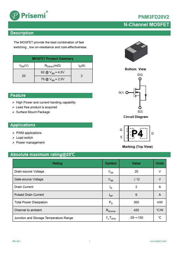
The MOSFET provide the best combination of fast switching , low on-resistance and cost-effectiveness.
MOSFET Product Summary
VDS(V) 20
RDS(on)(mΩ) 62 @ VGS = 4.5V 70 @ VGS = 2.5V
ID(A) 2
Feature
High Power and current handing capability Lead free product is acquired Surface Mount Package
Applications
PWM applications Load switch Power management
Absolute maximum rating@25℃
Rating Drain-source Voltage Gate-source Voltage Drain Current Pulsed Drain Current Total Power Dissipation Channel to ambient Junction and Storage Temperature Range
PNM3FD20V2 N-Channel MOSFET
Bottom View
D(3)
G(1)
S(2)
Circuit Diagram
P4 G D S
Marking (Top View)
Symbol VDS VGS ID IDP PD
Rth(ch-a) TJ,TSTG
Value 20
±12 2 6
300 420 -55~+150
Units V V A A
mW ℃/W
℃
Rev.06.1
1
www.