ELECTRICAL SPECIFICATIONS
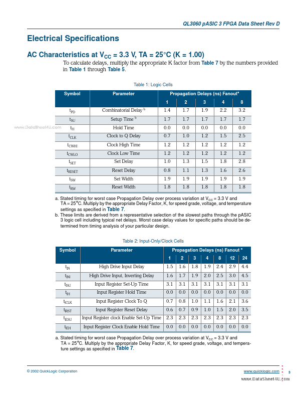
AC Characteristics at VCC = 3.3 V, TA = 25°C (K = 1.00) To calculate delays, multiply the appropriate K factor from Table 7 by the numbers provided in Table 1 through Table 5. Table 1: Logic Cells Symbol Parameter 1 tPD tSU Propagation Delays (ns) Fanouta 2 1.7 1.7 0.0 1.0 1.2 1.2 1.3 1.1 1.9 1.8 3 1.9 1.7 0.0 1.2 1.2 1.2 1.5 1.3 1.9 1.8 4 2.2 1.7 0.0 1.5 1.2 1.2 1.8 1.6 1.9 1.8 8 3.2 1.7 0.0 2.5 1.2 1.2 2.8 2.6 1.9 1.8 Combinatorial Delay Setup Time b Hold Time Clock to Q Delay Clock High Time Clock Low Time Set Delay Reset Delay Set Width Reset Width b 1.4 1.7 0.0 0.7 1.2 1.2 1.0 0.8 1.9 1.8 tH tCLK tCWHI tCWLO tSET tRESET tSW tRW a. Stated timing for worst case Propagation Delay over process variation at VCC = 3.3 V and TA = 25°C. Multiply by the appropriate Delay Factor, K, for speed grade, voltage, and temperature settings as specified in Table 7. b. These limits are derived from a representative selection of the slowest paths through the pASIC 3 logic cell including typical net delays. QuickLogic Corporation