RQK0604IGDQA Overview
Key Specifications
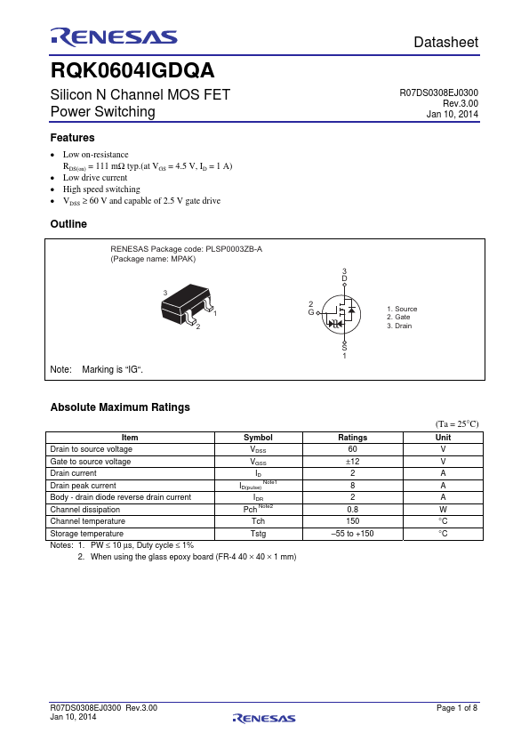
Pins: 3
Height: 1.4 mm
Length: 2 mm
Width: 3 mm
Key Features
- Low on-resistance RDS(on) = 111 mΩ typ.(at VGS = 4.5 V, ID = 1 A)
- Low drive current
- High speed switching
Pins: 3
Height: 1.4 mm
Length: 2 mm
Width: 3 mm
| Seller | Inventory | Price Breaks | Buy |
|---|---|---|---|
| Rochester Electronics | 1646 | 100+ : 0.3468 USD 500+ : 0.3121 USD 1000+ : 0.2878 USD 10000+ : 0.2566 USD |
View Offer |
| DigiKey Marketplace | 1646 | 692+ : 0.43 USD | View Offer |
| Part Number | Manufacturer | Description |
|---|---|---|
| RQK0609CQDQS | Renesas | N-Channel MOSFET |
| RQK0601AGDQS | Renesas | N-Channel MOSFET |
| RQK0607AQDQS | Renesas | N-Channel MOSFET |
| RQK0603CGDQS | Renesas | N-Channel MOSFET |
| RQK0608BQDQS | Renesas | N-Channel MOSFET |