Click to expand full text
www.DataSheet4U.com
RQK0606KGDQA
Silicon N Channel MOS FET Power Switching
REJ03G1497-0100 Rev.1.00 Jan 15, 2007
Features
• Low on-resistance RDS(on) = 173 mΩ typ.(at VGS = 4.5 V, ID = 0.8 A) • Low drive current • High speed switching • 
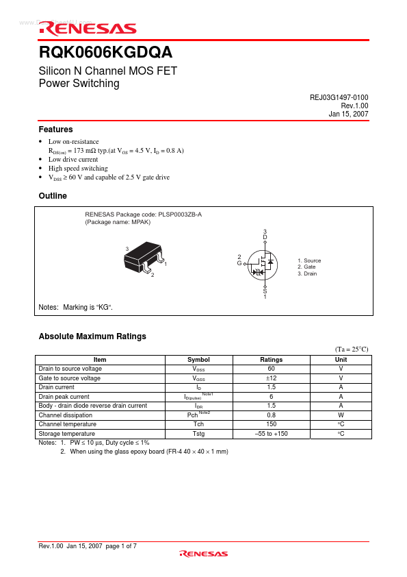
VDSS ≥ 60 V and capable of 2.5 V gate drive
Outline
RENESAS Package code: PLSP0003ZB-A (Package name: MPAK) 3 D
3 1 2
2 G
1. Source 2. Gate 3. Drain
S 1
Notes: Marking is “KG“.
Absolute Maximum Ratings
(Ta = 25°C)
Item Drain to source voltage Gate to source voltage Drain current Drain peak current Body - drain diode reverse drain current Channel dissipation Channel temperature Storage temperature Symbol VDSS VGSS ID ID(pulse) Note1 IDR Pch Note2 Tch Tstg Ratings 60 ±12 1.5 6 1.5 0.8 150 –55 to +150 Unit V V A A A W °C °C
Notes: 1.