ICS854S54I-01
ICS854S54I-01 is Differential-to-LVDS Multiplexer manufactured by Renesas.
Dual 2:1, 1:2 Differential-to-LVDS Multiplexer
Description
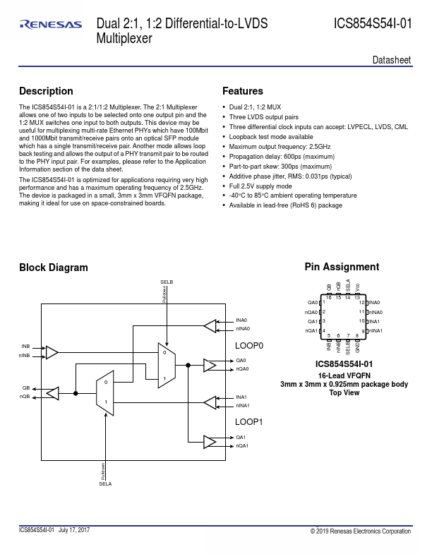
The ICS854S54I-01 is a 2:1/1:2 Multiplexer. The 2:1 Multiplexer allows one of two inputs to be selected onto one output pin and the 1:2 MUX switches one input to both outputs. This device may be useful for multiplexing multi-rate Ethernet PHYs which have 100Mbit and 1000Mbit transmit/receive pairs onto an optical SFP module which has a single transmit/receive pair. Another mode allows loop back testing and allows the output of a PHY transmit pair to be routed to the PHY input pair. For examples, please refer to the Application Information section of the data sheet.
The ICS854S54I-01 is optimized for...