ICS8752
ICS8752 is LVCMOS CLOCK MULTIPLIER/ZERO DELAY BUFFER manufactured by Renesas.
LOW SKEW, 1-TO-8 LVCMOS CLOCK MULTIPLIER/ZERO DELAY BUFFER
GENERAL DESCRIPTION
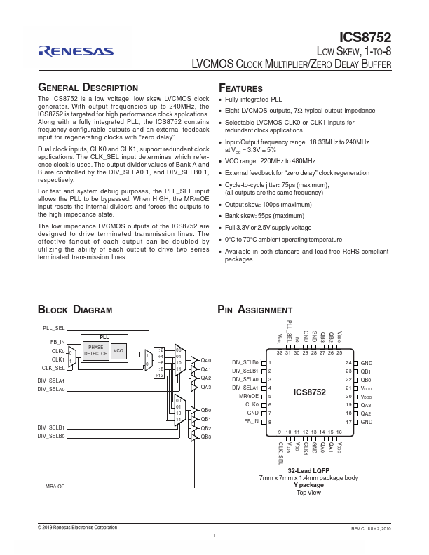
The ICS8752 is a low voltage, low skew LVCMOS clock generator. With output frequencies up to 240MHz, the ICS8752 is targeted for high performance clock applcations. Along with a fully integrated PLL, the ICS8752 contains frequency configurable outputs and an external feedback input for regenerating clocks with “zero delay”.
Dual clock inputs, CLK0 and CLK1, support redundant clock applications. The CLK_SEL input determines which reference clock is used. The output divider values of Bank A and B are controlled by the DIV_SELA0:1, and DIV_SELB0:1, respectively.
For test and system debug purposes, the PLL_SEL input allows the PLL to be bypassed. When HIGH, the MR/n OE input resets the internal dividers and forces the outputs to the high impedance state.
The low impedance LVCMOS outputs of the ICS8752 are designed to drive terminated transmission lines. The effective fanout of each output can be doubled by utilizing the ability of each output to drive two series terminated transmission lines.
Features
- Fully integrated PLL
- Eight LVCMOS outputs, 7Ω typical output impedance
- Selectable LVCMOS CLK0 or CLK1 inputs for redundant clock applications
- Input/Output frequency range: 18.33MHz to 240MHz at V = 3.3V ± 5%
- VCO range: 220MHz to 480MHz
- External feedback for “zero delay” clock regeneration
- Cycle-to-cycle jitter: 75ps (maximum), (all outputs are the same frequency)
- Output skew: 100ps (maximum)
- Bank skew: 55ps (maximum)
- Full 3.3V or 2.5V supply voltage
- 0°C to 70°C ambient operating temperature
- Available in both standard and lead-free Ro HS-pliant packages
BLOCK DIAGRAM
PLL_SEL
FB_IN CLK0 0 CLK1 1 CLK_SEL
DIV_SELA1 DIV_SELA0
PLL PHASE DETECTOR VCO
DIV_SELB1 DIV_SELB0
PIN ASSIGNMENT
VDDO QB2 QB3 GND GND nc PLL_SEL
÷2
1 ÷4
0...