ISLA224P
ISLA224P is Dual 14-Bit ADC manufactured by Renesas.
Features
- Single supply 1.8V operation
- Clock duty cycle stabilizer
- 75fs clock jitter
- 700MHz bandwidth
- Programmable built-in test patterns
- Multi-ADC support
- SPI programmable fine gain and offset control
- Support for multiple ADC synchronization
- Optimized output timing
- Nap and sleep modes
- 200µs sleep wake-up time
- Data output clock
- DDR LVDS-patible or LVCMOS outputs
- Selectable clock divider
Applications
- Radar array processing
- Software defined radios
- Broadband munications
- High-performance data acquisition
- munications test equipment
Pin-patible Family
MODEL ISLA224P20 ISLA224P13 ISLA222P25 ISLA222P20 ISLA222P13
RESOLUTION 14 14 12 12 12
SPEED (MSPS)
200 130 250 200 130
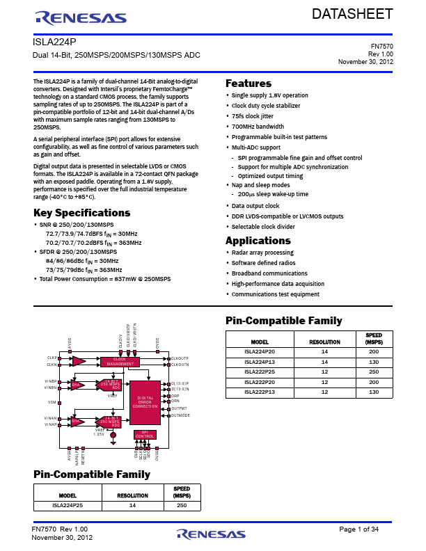
AVSS NAPSLP RESETN
CSB SCLK SDIO
SDO OVSS
Pin-patible Family
MODEL ISLA224P25
RESOLUTION 14
FN7570 Rev 1.00 November 30, 2012
SPEED (MSPS)
Page 1 of 34
Pin Configuration
- LVDS Mode
ISLA224P (72 LD QFN)
TOP...