RC22504A
RC22504A is Sub-100fs Frequency Synthesizer manufactured by Renesas.
Description
The RC22504A is a small, low-power timing ponent designed to be placed immediately adjacent to a PHY, switch, ASIC or FPGA that requires several reference clocks with jitter performance less than 100fs (max). The RC22504A can act as a frequency synthesizer to locally generate the reference clock or as a DCO for frequency margining or OTN clock applications.
The device is a member of Renesas' highperformance Femto Clock2 family.
Applications
- Reference clock generator for 100Gbps / 400Gbps PHYs or switches
- Adjustable OTN clock reference for OTU3 / OTU4 mappers
- Reference clock for programmable Fiber Optic Modules
Features
- Jitter as low as 64 fs RMS maximum (10k Hz to 20MHz)
- PLL core consists of fractional-feedback Analog PLL (APLL)
○ Operates from a 25MHz to 80MHz crystal or XO
○ APLL frequency independent of input / crystal frequency
○ Operates as a frequency synthesizer or Digitally Controlled Oscillator (DCO)
○ DCO has tuning granularity of < 1ppb
- Programmable status output
- 4 differential / 8 LVCMOS outputs
○ Any frequency from 10MHz to 1GHz (180MHz for LVCMOS)
○ Programmable output buffer supports HCSL (DC-coupled), LVDS/LVPECL/CML (AC-coupled) or two LVCMOS
○ Differential output swing is selectable: 400m V to 800m V
○ Output Enable input with programmable effect
- Supports up to 1MHz I2C or up to 20MHz SPI serial processor port
- Can configure itself automatically after reset via internal customer-definable One-Time Programmable (OTP) memory with up to four different configurations
- 4 × 4 mm 24-QFN package
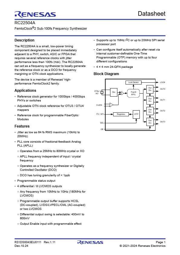
Block Diagram
XTAL/ XO
Osc
Lock Detect
Frac N APLL
CLKIN I2C / SPI
SEL OE
Registers
OT P
LOCK
Out Div
OUT0
Out Div
OUT1
Out Div
OUT2
Out...