Click to expand full text
Preliminary Datasheet
RQJ0303PGDQA
Silicon P Channel MOS FET Power Switching
Features
• Low on-resistance RDS(on) = 54 mΩ typ (VGS = –10 V, ID = –1.6 A) • Low drive current • High speed switching • 4.5 V gate drive R07DS0295EJ0600 Rev.6.00 Jan 10, 2014
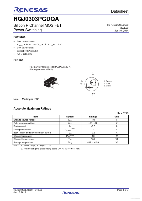
Outline
RENESAS Package code: PLSP0003ZB-A (Package name: MPAK)
3 D 3 G 1 2 S 1 2 1. Source 2. Gate 3. Drain
Note:
Marking is “PG”.
Absolute Maximum Ratings
(Ta = 25°C)
Item Drain to source voltage Gate to source voltage Drain current Drain peak current Body - drain diode reverse drain current Channel dissipation Channel temperature Storage temperature Symbol VDSS VGSS ID ID(Pulse) Note1 IDR Pch Note2 Tch Tstg Ratings –30 +10 / –20 –3.3 –5 –3.3 0.8 150 –55 to +150 Unit V V A A A W °C °C
Notes: 1. PW ≤ 10 μs, duty cycle ≤ 1% 2.