RQJ0304DQDQA
RQJ0304DQDQA is Silicon P-Channel MOS FET manufactured by Renesas.
Silicon P Channel MOS FET Power Switching
Features
- Low gate drive VDSS :
- 30 V and 2.5 V gate drive
- Low drive current
- High speed switching
- Small traditional package (MPAK)
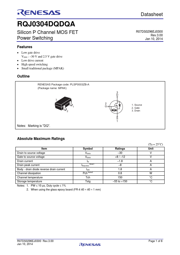
Outline
RENESAS Package code: PLSP0003ZB-A (Package name: MPAK)
1 2
Notes: Marking is "DQ".
Preliminary Datasheet
R07DS0296EJ0300 Rev.3.00
Jan 10, 2014
3 D
2 G
S 1
1. Source 2. Gate 3....