Datasheet4U Logo Datasheet4U.com

UPA2520 - MOS FIELD EFFECT TRANSISTOR

General Description

designed for DC/DC converter and power management applications of portable equipments.

Key Features

  • Low on-state resistance RDS(on)1 = 13.2 mΩ MAX. (VGS = 10 V, ID = 10 A) RDS(on)2 = 17 mΩ MAX. (VGS = 4.5 V, ID = 5.0 A).
  • Built-in gate protection diode.
  • Small and surface mount package (8-pin VSOF (2429)).
  • Pb-free (This product does not contain Pb in external electrode and other parts. ) 0 to 0.025 2.8±0.1 2.4±0.1 1 0.32±0.05 4 0.05 M S A (0.3) 1, 2, 3 : Source 4 : Gate 5, 6, 7, 8: Drain 0.8±0.05 S.

📥 Download Datasheet

Datasheet Details

Part number UPA2520
Manufacturer Renesas
File Size 292.54 KB
Description MOS FIELD EFFECT TRANSISTOR
Datasheet download datasheet UPA2520 Datasheet

Full PDF Text Transcription (Reference)

The following content is an automatically extracted verbatim text from the original manufacturer datasheet and is provided for reference purposes only.

View original datasheet text
DATA SHEET MOS FIELD EFFECT TRANSISTOR μ PA2520 N-CHANNEL MOS FET FOR SWITCHING DESCRIPTION The μ PA2520 is N-channel MOS Field Effect Transistor designed for DC/DC converter and power management applications of portable equipments. 
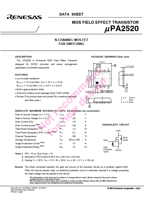
PACKAGE DRAWING (Unit: mm) 2.9±0.1 0.65 8 5 A 0.17±0.05 FEATURES • Low on-state resistance RDS(on)1 = 13.2 mΩ MAX. (VGS = 10 V, ID = 10 A) RDS(on)2 = 17 mΩ MAX. (VGS = 4.5 V, ID = 5.0 A) • Built-in gate protection diode • Small and surface mount package (8-pin VSOF (2429)) • Pb-free (This product does not contain Pb in external electrode and other parts.) 0 to 0.025 2.8±0.1 2.4±0.1 1 0.32±0.05 4 0.05 M S A (0.3) 1, 2, 3 : Source 4 : Gate 5, 6, 7, 8: Drain 0.8±0.05 S ABSOLUTE MAXIMUM RATINGS (TA = 25°C, All terminals are connected.