Datasheet4U Logo Datasheet4U.com

BU2090 - serial-IN/parallel-OUT driver

Datasheet Summary

Description

Pin No.

4 5 6 7 8 9 10 11 12 13 14 15 16 BU2092 / F BU2092 / FV 1 2 3 4 5 6 7 8 9 10 11

12 13 14 15 16 17 18 1 2 3 4 5 6 7 8 9 10 11 12 13 14 15 16 17 18 19 20 Pin name VSS DATA CLOCK LCK Q0 Q1 Q2 Q3 Q4 Q5 Q6 N.C.

Features

  • 1) Low power dissipation. 2) Operating voltages ranging from 2.7 to 5.5V. 3) Output is Nch open drain. 4) High output withstand voltage of + 25V. 5) Diverse variety of packages. BU2090 / F / FS: DIP16, SOP16, SSOP-A16 BU2092 / F / FV: DIP18, SOP18, SSOP-A18 (plastic molds) 6) High drive capability; direct lighting of green LED possible. 1 Standard ICs maximum ratings (Ta = 25°C).
  • Absolute (BU2090 / F / FS, BU2092 / F / FV) Parameter Power supply voltage Power dissipation Pow.

📥 Download Datasheet

Datasheet preview – BU2090

Datasheet Details

Part number BU2090
Manufacturer ROHM
File Size 140.34 KB
Description serial-IN/parallel-OUT driver
Datasheet download datasheet BU2090 Datasheet
Additional preview pages of the BU2090 datasheet.
Other Datasheets by Rohm

Full PDF Text Transcription

Click to expand full text
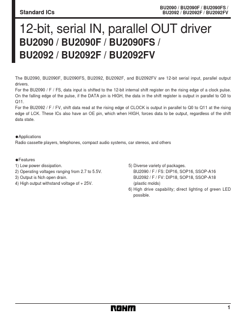
Standard ICs BU2090 / BU2090F / BU2090FS / BU2092 / BU2092F / BU2092FV 12-bit, serial IN, parallel OUT driver BU2090 / BU2090F / BU2090FS / BU2092 / BU2092F / BU2092FV The BU2090, BU2090F, BU2090FS, BU2092, BU2092F, and BU2092FV are 12-bit serial input, parallel output drivers. For the BU2090 / F / FS, data input is shifted to the 12-bit internal shift register on the rising edge of a clock pulse. On the falling edge of the pulse, if the DATA pin is HIGH, the data in the shift register is output in parallel to Q0 to Q11. For the BU2092 / F / FV, shift data read at the rising edge of CLOCK is output in parallel to Q0 to Q11 at the rising edge of LCK. These ICs also have an OE pin, which when HIGH, forces data to be output, regardless of the shift data state.
Published: |