MS90C365
MS90C365 is Flat Panel Display Transmitter manufactured by Ruimeng.
Description
The MS90C365 transmitter converts 21 bits of LVCMOS/LVTTL data into four LVDS (Low Voltage Differential Signaling) data streams. A phase-locked transmit clock is transmitted in parallel with the data streams. At a transmit clock frequency of 150MHz, 18 bits of RGB data and 3 bits of LCD timing and control data are transmitted at a rate of 1050 Mbps per LVDS data channel. Using a 150 MHz clock, the data throughput is 525 Mbytes/sec. The MS90C365 can be programmed for Rising edge strobe or Falling edge strobe through the R_FB pin.
This chipset is an ideal means to solve EMI and cable size problems associated with wide, high-speed TTL interfaces.
Features
- Frequency Range:20-150MHz
- Single Supply:3.3V
- I/O power supply patible with 1.8V, 3.3V
- Power-down mode < 200µW (max)
- Supports VGA, SVGA, XGA and Dual Pixel SXGA.
- Up to 525 Megabytes/sec bandwidth
- reduced swing LVDS to reduce EMI(200m V or 345m V Optional)
- Internal PLL
- Low profile 48 lead TSSOP package
- patible with TIA/EIA-644 LVDS standard
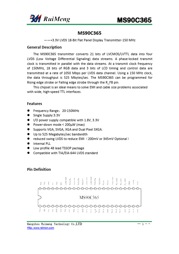
Pin Definition
Hangzhou Ruimeng Technology Co.,LTD
Http: .relmon.
-- 1
- -
MS90C365 Pin Description
Pin name TXOUT0-,TXOUT0+ TXOUT1-, TXOUT1+ TXOUT2-, TXOUT2+
TCLK+, TCLKTX0 ~ TX6 TX7 ~ TX13 TX14 ~ TX20 CLK IN /PDN R_FB
RS VCC I/O VCC
GND LVDS VCC LVDS GND PLL VCC PLL GND
Pin number 40, 41 38, 39 34, 35 32, 33
44,45,47,48,1,3,4 6,7,9,10,12,1315 16,18,19,20,22,23,
25 26 27 14
2 8 21
5,11,17,24,46 37
31,36,42 29
28,30 type LVDS outputs LVDS outputs LVDS outputs LVDS outputs inputs inputs inputs inputs inputs inputs inputs
Power supply
I/O power supply Ground Power supply
Ground
Power supply Ground
Description
LVDS differential data output
LVDS differential clock output
TTL TTL level input include:8 RED,8 GREEN,8
BLUE,4 control lines(HSYNC,VSYNC,DE,CNTL)...