Download IRF630M Datasheet PDF
STMicroelectronics
IRF630M
IRF630M is N-Channel MOSFET manufactured by STMicroelectronics.
DESCRIPTION 
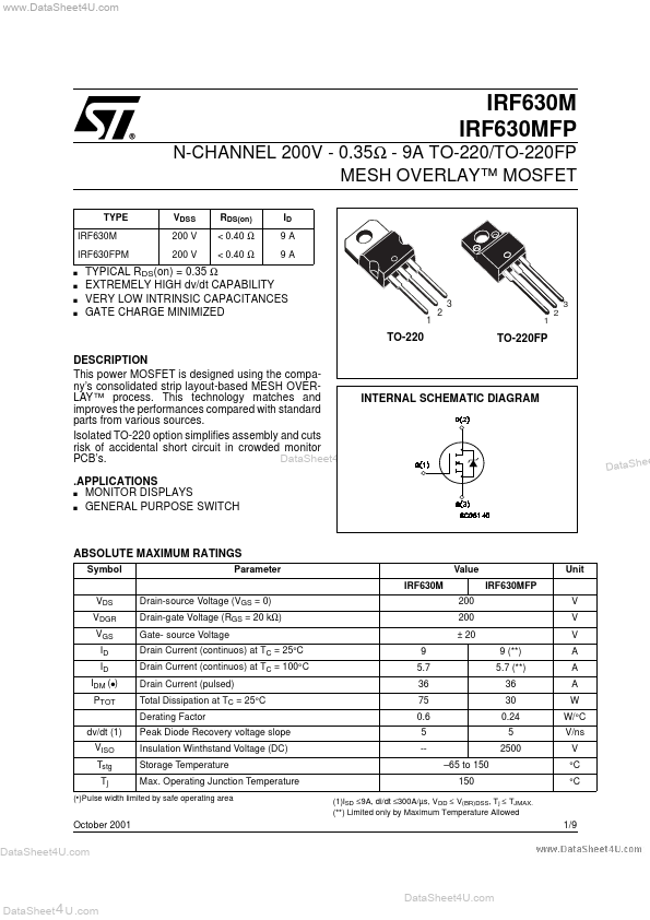
This power MOSFET is designed using the pany’s consolidated strip layout-based MESH OVERLAY™ process. This technology matches and INTERNAL SCHEMATIC DIAGRAM improves the performances pared with standard parts from various sources. Isolated TO-220 option simplifies assembly and cuts risk of accidental short circuit in crowded monitor PCB’s. . .APPLICATIONS s MONITOR DISPLAYS s GENERAL PURPOSE SWITCH Data Sh ee ABSOLUTE MAXIMUM RATINGS Symbol VDS VDGR VGS ID ID IDM (q) PTOT dv/dt (1) VISO Tstg Tj Parameter IRF630M Drain-source Voltage (VGS = 0) Drain-gate Voltage (RGS = 20 kΩ) Gate- source Voltage Drain Current (continuos) at TC = 25°C Drain Current (continuos) at TC = 100°C Drain Current (pulsed) Total Dissipation at TC = 25°C Derating Factor Peak Diode Recovery voltage slope Insulation Winthstand Voltage (DC) Storage Temperature Max. Operating Junction Temperature 9 5.7 36 75 0.6 5 -- 65 to 150 150 (1)ISD ≤9A, di/dt ≤300A/µs, V DD ≤ V(BR)DSS, Tj ≤ TJMAX. (- - ) Limited only by Maximum Temperature Allowed Value IRF630MFP 200 200 ± 20 9 (- - ) 5.7 (- - ) 36 30 0.24 5 2500 Unit V V V A A A W W/°C V/ns V °C °C (- )Pulse width limited by safe operating area October 2001 1/9 . . Data Sheet 4 U . .. IRF630M / FP THERMAL DATA TO-220 Rthj-case Rthj-amb Tl Thermal Resistance Junction-case Max Thermal Resistance Junction-ambient Max Maximum Lead Temperature For Soldering Purpose 1.67 62.5 300 TO-220FP 4.17 °C/W °C/W °C ELECTRICAL CHARACTERISTICS (TCASE = 25 °C UNLESS OTHERWISE SPECIFIED) OFF Symbol V(BR)DSS IDSS IGSS Parameter Drain-source Breakdown Voltage Zero Gate Voltage Drain Current (VGS = 0) Gate-body Leakage Current (VDS = 0) Test Conditions ID = 250 µA, VGS = 0 VDS = Max Rating VDS = Max Rating, TC = 125 °C VGS = ± 20V Min. 200 1 50 ±100 Typ. Max. Unit V µA µA n A ON (1) Symbol VGS(th) RDS(on) Parameter Gate Threshold Voltage Static Drain-source On Resistance Test Conditions VDS = VGS, ID = 250µA VGS = 10V, ID = 4.5 A Min. 2 Typ. 3 0.35 Max. 4 0.40...