STB80NE03L-06
STB80NE03L-06 is N-CHANNEL POWER MOSFET manufactured by STMicroelectronics.
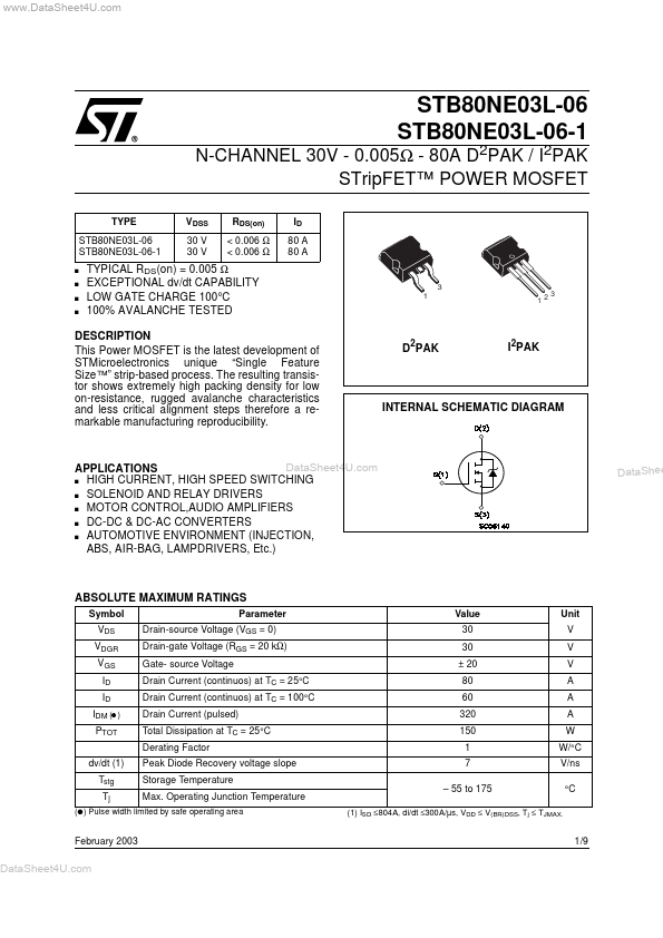
DESCRIPTION
This Power MOSFET is the latest development of STMicroelectronics unique “Single Feature
Size™” strip-based process. The resulting transistor shows extremely high packing density for low on-resistance, rugged avalanche characteristics and less critical alignment steps therefore a remarkable manufacturing reproducibility.
D2PAK
I2PAK
INTERNAL SCHEMATIC DIAGRAM
. APPLICATIONS HIGH CURRENT, HIGH SPEED SWITCHING s SOLENOID AND RELAY DRIVERS s MOTOR CONTROL,AUDIO AMPLIFIERS s DC-DC & DC-AC CONVERTERS s AUTOMOTIVE ENVIRONMENT (INJECTION, ABS, AIR-BAG, LAMPDRIVERS, Etc.) s
Data Shee
ABSOLUTE MAXIMUM RATINGS
Symbol VDS VDGR VGS ID ID IDM ( ) PTOT dv/dt (1) Tstg Tj Parameter Drain-source Voltage (VGS = 0) Drain-gate Voltage (RGS = 20 kΩ) Gate- source Voltage Drain Current (continuos) at TC = 25°C Drain Current (continuos) at TC = 100°C Drain Current (pulsed) Total Dissipation at TC = 25°C Derating Factor Peak Diode Recovery voltage slope Storage Temperature Max. Operating Junction Temperature Value 30 30 ± 20 80 60 320 150 1 7
- 55 to 175
(1) ISD ≤ 804A, di/dt ≤300A/µs, VDD ≤ V(BR)DSS, T j ≤ TJMAX.
Unit V V V A A A W W/°C V/ns °C
(q ) Pulse width limited by safe operating area
February 2003
1/9
.
..
STB80NE03L-06 / STB80NE03L-06-1
THERMAL DATA
Rthj-case Rthj-amb Tl Thermal Resistance Junction-case Max Thermal Resistance Junction-ambient Max Maximum Lead Temperature For Soldering Purpose 1 62.5 300 °C/W °C/W °C
AVALANCHE CHARACTERISTICS
Symbol IAR EAS Parameter Avalanche Current, Repetitive or Not-Repetitive (pulse width limited by Tj max) Single Pulse Avalanche Energy (starting Tj = 25 °C, ID = IAR, VDD = 15 V) Max Value 80 600 Unit A m J
ELECTRICAL CHARACTERISTICS (TCASE = 25 °C UNLESS OTHERWISE SPECIFIED) OFF
Symbol V(BR)DSS IDSS IGSS Parameter Drain-source Breakdown Voltage Zero Gate Voltage Drain Current (VGS = 0) Gate-body Leakage Current (VDS = 0) Test Conditions ID = 250 µA, VGS = 0 VDS = Max Rating VDS = Max Rating, TC = 125 °C VGS = ± 20 V...