STW220NF75
STW220NF75 is N-CHANNEL POWER MOSFET manufactured by STMicroelectronics.
DESCRIPTION
This Power MOSFET is the latest development of STMicroelectronis unique "Single Feature
Size™" stripbased process. The resulting transistor shows extremely high packing density for low on-resistance, rugged avalanche characteristics and less critical alignment steps therefore a remarkable manufacturing reproducibility.
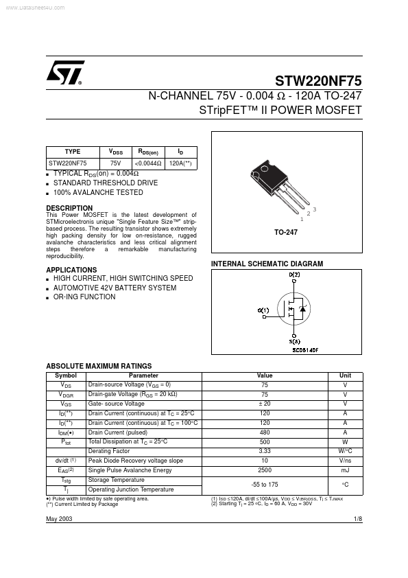
TO-247
APPLICATIONS s HIGH CURRENT, HIGH SWITCHING SPEED s AUTOMOTIVE 42V BATTERY SYSTEM s OR-ING FUNCTION
INTERNAL SCHEMATIC DIAGRAM
ABSOLUTE MAXIMUM RATINGS
Symbol VDS VDGR VGS ID(-
- ) ID(-
- ) IDM(- ) Ptot dv/dt (1) EAS(2) Tstg Tj Parameter Drain-source Voltage (VGS = 0) Drain-gate Voltage (RGS = 20 kΩ) Gate- source Voltage Drain Current (continuous) at TC = 25°C Drain Current (continuous) at TC = 100°C Drain Current (pulsed) Total Dissipation at TC = 25°C Derating Factor Peak Diode Recovery voltage slope Single Pulse Avalanche Energy Storage Temperature Operating Junction Temperature Value 75 75 ± 20 120 120 480 500 3.33 10 2500 -55 to 175 Unit V V V A A A W W/°C V/ns m J °C
- ) Pulse width limited by safe operating area. (-
- ) Current Limited by Package
May 2003
(1) ISD ≤120A, di/dt ≤100A/µs, VDD ≤ V (BR)DSS, T j ≤ TJMAX (2) Starting T j = 25 o C, ID = 60 A, VDD = 30V
1/8
THERMAL DATA
Rthj-case Rthj-amb Tj Thermal Resistance Junction-case Thermal Resistance Junction-ambient Maximum Lead Temperature For Soldering Purpose (1.6 mm from case, for 10 sec) Max Max Typ 0.30 50 300 °C/W °C/W °C
ELECTRICAL CHARACTERISTICS (Tcase = 25 °C unless otherwise specified) OFF
Symbol V(BR)DSS IDSS Parameter Drain-source Breakdown Voltage Zero Gate Voltage Drain Current (VGS = 0) Gate-body Leakage Current (VDS = 0) Test Conditions ID = 250 µA, VGS = 0 VDS = Max Rating VDS = Max Rating TC = 125°C VGS = ± 20V Min. 75 1 10 ±100 Typ. Max. Unit V µA µA n A
IGSS
ON (1)
Symbol VGS(th) RDS(on) Parameter Gate Threshold Voltage Static Drain-source On Resistance Test Conditions VDS = VGS VGS = 10 V ID = 250 µA ID = 60 A Min. 2 0.004 Typ. Max....