Datasheet4U Logo Datasheet4U.com

74VHCT05A Datasheet Hex Inverter

Manufacturer: STMicroelectronics

Overview: ® 74VHCT05A HEX INVERTER (OPEN DRAIN) s s s s s s s s HIGH SPEED: tPD = 3.2 ns (TYP.) at VCC = 5V LOW POWER DISSIPATION: ICC = 2 µA (MAX.) at TA = 25 oC PATIBLE WITH TTL OUTPUTS: VIH = 2V (MIN), VIL = 0.8V (MAX) POWER DOWN PROTECTION ON INPUTS OPERATING VOLTAGE RANGE: VCC (OPR) = 4.5V to 5.5V PIN AND FUNCTION PATIBLE WITH 74 SERIES 05 IMPROVED LATCH-UP IMMUNITY LOW NOISE: VOLP = 0.8V (Max.) M (Micro Package) T (TSSOP Package) ORDER CODES : 74VHCT05AM 74VHCT05AT Power down protection is provided on all inputs and 0 to 7V can be accepted on inputs with no regard to the supply voltage. This device can be used to interface 5V to 3V. All inputs and outputs are equipped with protection circuits against static discharge, giving them 2KV ESD immunity and transient excess voltage.

General Description

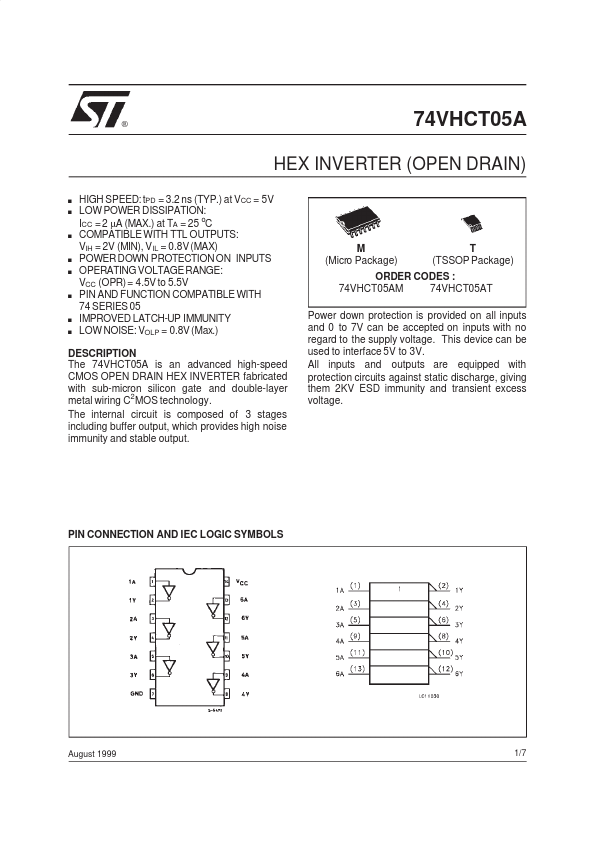
The 74VHCT05A is an advanced high-speed CMOS OPEN DRAIN HEX INVERTER fabricated with sub-micron silicon gate and double-layer metal wiring C2MOS technology.

The internal circuit is posed of 3 stages including buffer output, which provides high noise immunity and stable output.

PIN CONNECTION AND IEC LOGIC SYMBOLS August 1999 1/7 74VHCT05A INPUT EQUIVALENT CIRCUIT PIN DESCRIPTION PIN No 1, 3, 5, 9, 11, 13 2, 4, 6, 8, 10, 12 7 14 SYMBOL 1A to 6A 1Y to 6Y GND VCC NAME AND FUNCT ION Data Inputs Data Outputs Ground (0V) Positive Supply Voltage TRUTH TABLE A L H Z: High Impedance Y Z L ABSOLUTE MAXIMUM RATINGS Symbol VCC VI VO IIK IOK IO Tstg TL Supply Voltage DC Input Voltage DC Output Voltage DC Input Diode Current DC Output Diode Current DC Output Current Storage Temperature Lead Temperature (10 sec) Parameter Value -0.5 to +7.0 -0.5 to +7.0 -0.5 to VCC + 0.5 - 20 ± 20 25 ± 50 -65 to +150 300 Unit V V V mA mA mA mA o o ICC or IGND DC VCC or Ground Current C C Absolute Maximum Ratings are those values beyond which damage to the device may occur.

74VHCT05A Distributor