Datasheet4U.com
🌙
PSD813F1-A Datasheet | STMicroelectronics
Part:
PSD813F1-A
Description:
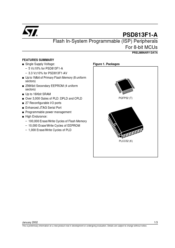
Flash In-System Programmable (ISP) Peripherals
Manufacturer:
STMicroelectronics
Size:
553.43 KB
PSD813F1-A Datasheet (PDF) Download
Related PSD813F1-A Datasheets
PSD813F1 Flash In-System Programmable Peripherals
PSD813F1V Flash in-system programmable peripherals
PSD813F1A Flash in-system programmable (ISP) peripherals
PSD813F2 Flash in-system programmable (ISP) peripherals for 8-bit MCUs
PSD813F4 Flash in-system programmable (ISP) peripherals for 8-bit MCUs
STMicroelectronics
PSD813F1-A
Key Features
SUMMARY s Single Supply Voltage
×
Close