STMicroelectronics STY80NM60N
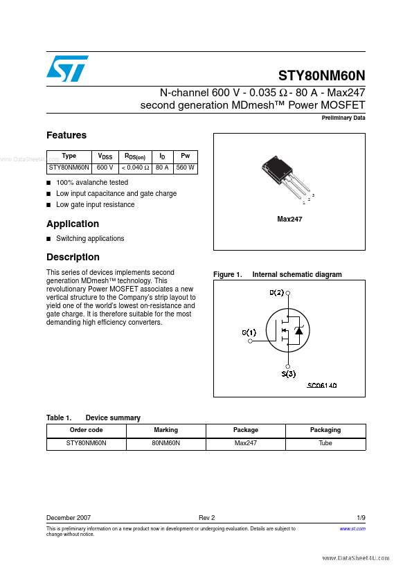
This series of devices implements second generation MDmesh™ technology. This revolutionary Power MOSFET associates a new vertical structure to the Company’s strip layout to yield one of the world’s lowest on-resistance and gate charge.| Part No. | STY80NM60N |
|---|---|
| Datasheet | STY80NM60N Download |
| Manufacturer |  STMicroelectronics |
| Description | N-channel Power MOSFET |
| Buy | Stock & Price |
FEATURES
Type VDSS 600 V RDS(on) < 0.040 Ω ID 80 A Pw 560 W STY80NM60N●
●
● 100% avalanche tested Low input capacitance and gate charge Low gate input resistance Max247 1 2 3 Application
● Switching applications
DESCRIPTION
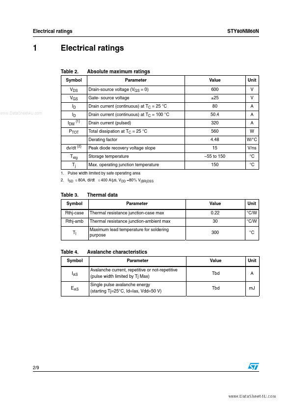
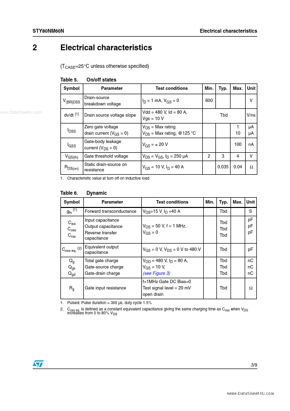
It is therefore suitable for the most demanding high efficiency converters. Figure 1. Internal schematic diagram Table 1. Device summary Marking 80NM60N Package Max247 Packaging Tube Order code STY80NM60N December 2007 Rev 2 1/9 9 This is preliminary information on a new product now in development or undergoing evaluation. Details are subject to change without notice. Electrical ratings STY80NM60N 1 Electrical ratings Table 2. Symbol VDS VGS ID Absolute maximum ratings Parameter Drain-source voltage (VGS = 0) Gate- source voltage Drain current (continuous) at TC = 25 °C Drain current (continuous) at TC = 100 °C Drain current (pulsed) Total dissipation at TC = 25 °C Derating factor Value 600 ±25 80 50.4 320 560 4.48 15 –55 to 150 150 Unit V V A A A W W/°C V/ns °C °C ID IDM (1) PTOT dv/dt (2) Tstg Tj Peak diode recovery voltage slope Storage temperature Max. operating junction temperature 1.