STMicroelectronics VND10B
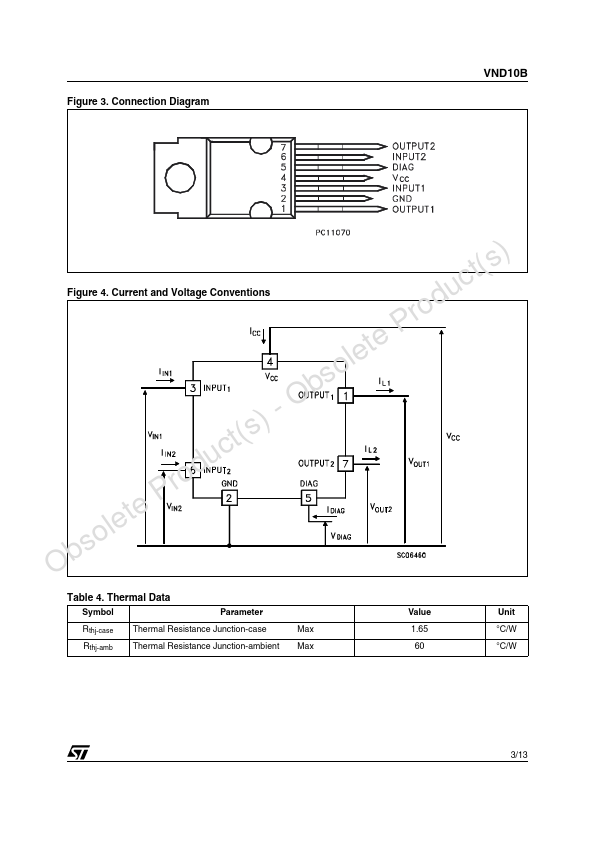
VND10B is a monolithic device made using dSTMicroelectronics VIPower Technology, rointended for driving resistive or inductive loads Pwith one side grounded. This device has two channels, and a common diagnostic.| Part No. | VND10B |
|---|---|
| Datasheet | VND10B Download |
| Manufacturer |  STMicroelectronics |
| Description | DOUBLE CHANNEL HIGH SIDE SMART POWER SOLID STATE RELAY |
| Buy | Stock & Price |
GENERAL FEATURES
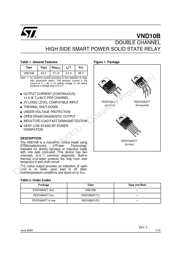
Figure 1. Package Type VDSS RDS(on) In(1) VCC VND10B 40 V 0.1 Ω 3.4 A 26 V )Note: 1. In= Nominal current according to ISO definition for high t(sside automotive switch. The Nominal Current is the current at Tc = 85 °C for battery voltage of 13V which produces a voltage drop of 0.5 V. duc● OUTPUT CURRENT (CONTINUOUS): ro14 A @ Tc=85°C PER CHANNEL P● 5V LOGIC LEVEL COMPATIBLE INPUT te● THERMAL SHUT-DOWN le● UNDER VOLTAGE PROTECTION so● OPEN DRAIN DIAGNOSTIC OUTPUT b● INDUCTIVE LOAD FAST DEMAGNETIZATION - O● VERY LOW STAND-BY POWER )DISSIPATION ct(sDESCRIPTION uThe Built-in tethermal shut-down protects the chip from over letemperature and short circuit. oThe stat