VNS1NV04
DESCRIPTION
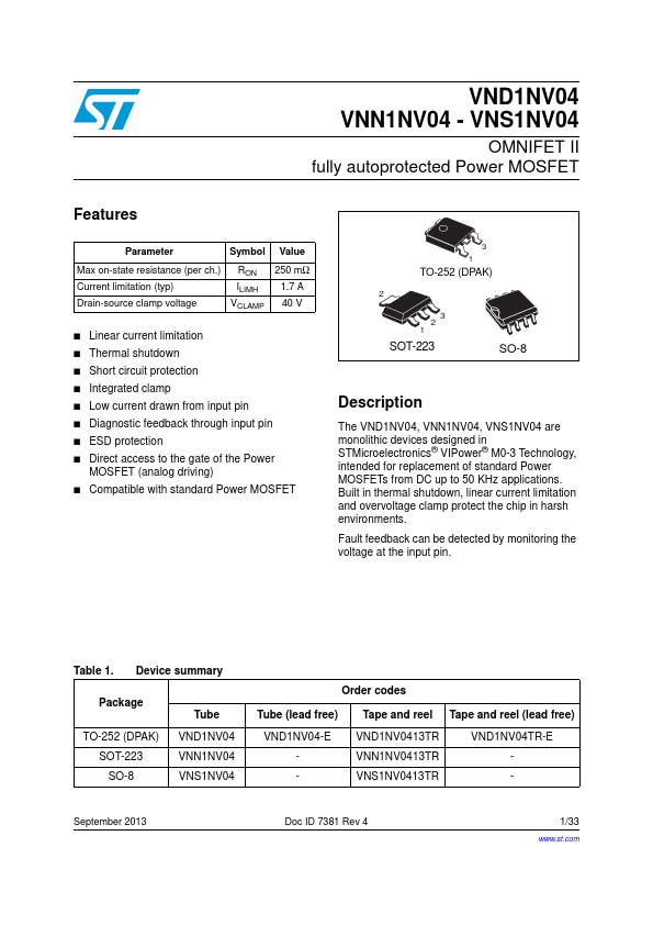
The VND1NV04, VNN1NV04, VNS1NV04 are monolithic devices designed in STMicroelectronics VIPower M0-3 Technology, intended for replacement of standard Power BLOCK DIAGRAM
MOSFETS from DC up to 50KHz applications. Built in thermal shutdown, linear current limitation and overvoltage clamp protect the chip in harsh environments. Fault feedback can be detected by monitoring the voltage at the input pin.
DRAIN
2 Overvoltage Clamp
INPUT
Gate Control
Over Temperature
Linear Current Limiter
SOURCE
FC01000
February 2003
1/18
VND1NV04 / VNN1NV04 / VNS1NV04
ABSOLUTE MAXIMUM RATING
Symbol VDS VIN IIN RIN MIN ID IR VESD1 VESD2 Ptot Tj Tc Tstg Parameter Drain-source Voltage (VIN=0V) Input Voltage Input Current Minimum Input Series Impedance Drain Current Reverse DC Output Current Electrostatic Discharge (R=1.5KΩ, C=100p F) Electrostatic Discharge on output pin only (R=330Ω, C=150p F) Total Dissipation at Tc=25°C Operating Junction Temperature Case Operating Temperature...