VNS1NV04D
DESCRIPTION
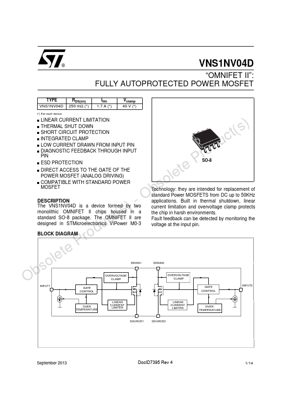
The VNS1NV04D is a device formed by two monolithic OMNIFET II chips housed in a standard SO-8 package. The OMNIFET II are designed in STMicroelectronics VIPower M0-3 BLOCK DIAGRAM
..
Technology: they are intended for replacement of standard Power MOSFETS from DC up to 50KHz applications. Built in thermal shutdown, linear current limitation and overvoltage clamp protects the chip in harsh environments. Fault feedback can be detected by monitoring the voltage at the input pin.
DRAIN1
DRAIN2
OVERVOLTAGE CLAMP INPUT1 GATE CONTROL
OVERVOLTAGE CLAMP GATE CONTROL INPUT2
OVER TEMPERATURE
LINEAR CURRENT LIMITER
LINEAR CURRENT LIMITER
OVER TEMPERATURE
SOURCE1
SOURCE2
February 2003
1/14
ABSOLUTE MAXIMUM RATING
Symbol VDSn VINn IINn RIN MINn IDn IRn VESD1 VESD2 Ptot Tj Tc Tstg Parameter Drain-source Voltage (VINn=0V) Input Voltage Input Current Minimum Input Series Impedance Drain Current Reverse DC Output Current Electrostatic Discharge (R=1.5KΩ, C=100p F)...