SDD3055L2
SDD3055L2 is N-Channel E nhancement Mode Field Effect Transistor manufactured by SamHop Microelectronics.
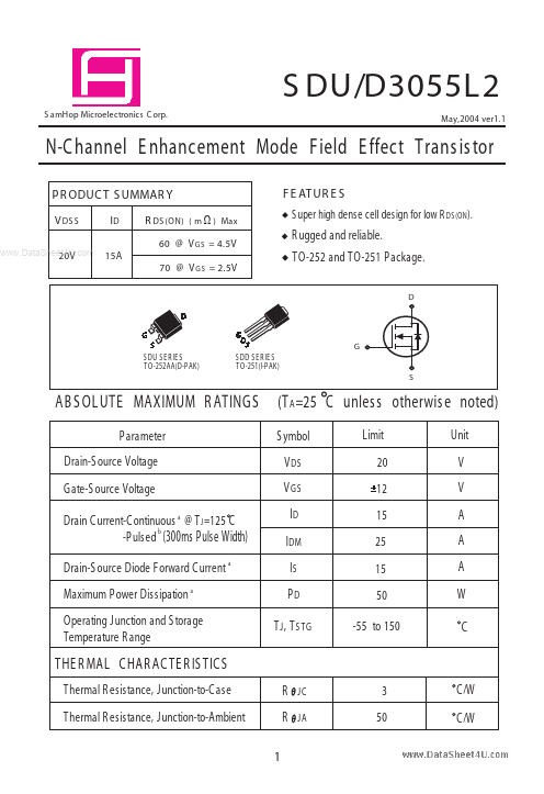
S DU/D3055L2
S am Hop Microelectronics C orp. May,2004 ver1.1
N-C hannel E nhancement Mode Field E ffect Trans is tor
P R ODUC T S UMMAR Y
V DS S
.. 20V
F E AT UR E S
( m W ) Max
15A
R DS (ON)
S uper high dense cell design for low R DS (ON ).
60 @ V G S = 4.5V 70 @ V G S = 2.5V
R ugged and reliable. TO-252 and TO-251 P ackage.
S DU S E R IE S TO-252AA(D-P AK)
S DD S E R IE S TO-251(l-P AK)
AB S OL UTE MAXIMUM R ATINGS
P arameter Drain-S ource Voltage Gate-S ource Voltage Drain C urrent-C ontinuous a @ T J =125 C b -P ulsed (300ms Pulse Width) Drain-S ource Diode Forward C urrent a Maximum P ower Dissipation a Operating Junction and S torage Temperature R ange
(T A =25 C unles s otherwis e noted)
S ymbol V DS V GS ID IDM IS PD T J , T S TG Limit 20 12 15 25 15 50 -55 to 150 Unit V V A A A W C
THE R MAL C HAR AC TE R IS TIC S
Thermal R esistance, Junction-to-C ase Thermal R esistance, Junction-to-Ambient
R JC R JA
3 50
C /W C /W
S DU/D3055L2
E LE CTR ICAL CHAR ACTE R IS TICS (T A =25 C unless otherwise noted)
Parameter OFF CHAR ACTE R IS TICS
Drain-S ource Breakdown Voltage Zero Gate Voltage Drain Current
..
S ymbol
BV DS S IDS S IGS S V GS (th) R DS (ON) ID(ON) g FS C IS S C OS S CRSS c
Condition
V GS = 0V, ID = 250u A V DS = 20V, V GS = 0V V GS = 8V, V DS = 0V V DS = V GS , ID = 250u A V GS =4.5V, ID = 6.0A V GS =2.5V, ID = 5.2A V DS = 5V, V GS = 4.5V V DS = 10V, ID = 6.0A
Min Typ C Max Unit
20 1 100 0.7 34 45 20 17 705 280 65 60 70 V u A n A V m-ohm...