SDD30N02
SDD30N02 is N-Channel E nhancement Mode Field Effect Transistor manufactured by SamHop Microelectronics.
S DU/D30N02
S am Hop Microelectronics C orp. May,2004 ver1.1
N-C hannel E nhancement Mode Field E ffect Transistor
P R ODUC T S UMMAR Y
V DS S
.. 20V
F E AT UR E S S uper high dense cell design for low R DS (ON ).
25A
R DS (ON) ( m W ) Max
20 @ V G S = 4.5V
R ugged and reliable. TO-252 and TO-251 P ackage.
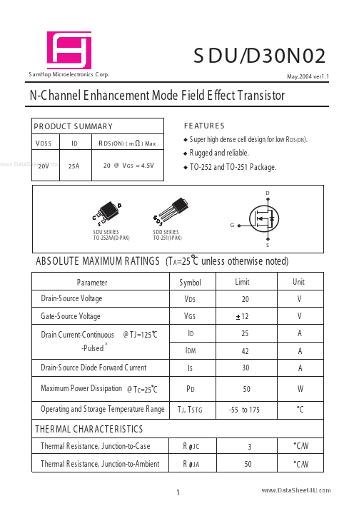
S DU S E R IE S TO-252AA(D-P AK)
S DD S E R IE S TO-251(l-P AK)
ABS OLUTE MAXIMUM R ATINGS (T A=25 C unless otherwise noted)
P arameter Drain-S ource Voltage Gate-S ource Voltage Drain C urrent-C ontinuous -P ulsed a
S ymbol V DS V GS @ TJ=125 C ID IDM IS PD T J , T S TG
Limit 20 12 25 42 30 50 -55 to 175
Unit V V A A A W C
Drain-S ource Diode Forward C urrent Maximum P ower Dissipation @ Tc=25 C Operating and S torage Temperature R ange
THE R MAL C HAR AC TE R IS TIC S
Thermal R esistance, Junction-to-C ase Thermal R esistance, Junction-to-Ambient
R JC R JA
3 50
C /W C /W
S DU/D30N02
E LE CTR ICAL CHAR ACTE R IS TICS (T C =25 C unless otherwise noted)
Parameter OFF CHAR ACTE R IS TICS
Drain-S ource Breakdown Voltage
..
S ymbol
BV DS S IDS S IGS S V GS (th) R DS (ON) ID(ON) g FS b
Condition
V GS = 0V, ID = 250u A V DS = 16V, V GS = 0V V GS = 8V, V DS = 0V V DS = V GS , ID = 250u A V GS = 4.5V, ID = 20A V DS = 10V, V GS = 4.5V V DS = 10V, ID = 20A
Min Typ Max Unit
20...