STS2309A Overview
Key Features
- 20 1 100 -0.5 -0.8 -1.5 115 175 -5 6 290 60 45 130 190 V uA nA V
| Part | STS2309A |
|---|---|
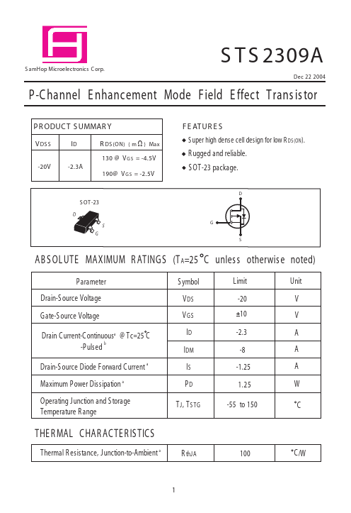
| Description | P -Channel Enhancement Mode Field Effect Transistor |
| Category | Transistor |
| Manufacturer | SamHop Microelectronics |
| Size | 720.22 KB |
| Part Number | Manufacturer | Description |
|---|---|---|
| STS2309A | VBsemi | P-Channel MOSFET |
| STS2301 | VBsemi | P-Channel 20V MOSFET |