KM23C8105D
KM23C8105D is 8M-Bit (1Mx8 /512Kx16) CMOS Mask ROM manufactured by Samsung Semiconductor.
FEATURES
- Switchable organization 1,048,576 x 8(byte mode) 524,288 x 16(word mode)
- Fast access time Random Access : 100ns(Max.) Page Access : 30ns(Max.)
- 4 Words / 8 bytes page access
- Supply voltage : single +5V
- Current consumption Operating : 80m A(Max.) Standby : 50µA(Max.)
- Fully static operation
- All inputs and outputs TTL patible
- Three state outputs
- Package -. KM23C8105D : 42-DIP-600 -. KM23C8105DG : 44-SOP-600
CMOS MASK ROM
GENERAL DESCRIPTION
The KM23C8105D(G) is a fully static mask programmable ROM fabricated using silicon gate CMOS process technology, and is organized either as 1,048,576 x 8 bit(byte mode) or as 524,288 x 16 bit(word mode) depending on BHE voltage level.(See mode selection table) This device includes page read mode function, page read mode allows 4 words (or 8bytes) of data to read fast in the same page, CE and A 2 ~ A18 should not be changed. This device operates with a 5V single power supply, and all inputs and outputs are TTL patible. Because of its asynchronous operation, it requires no external clock assuring extremely easy operation. It is suitable for use in program memory of microprocessor, and data memory, character generator. The KM23C8105D is packaged in a 42-DIP and the KM23C8105DG in a 44-SOP.
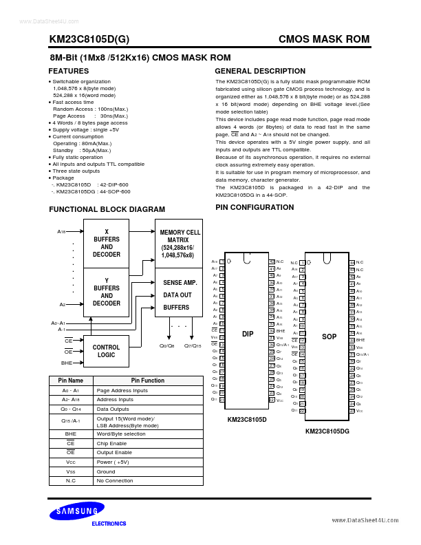
FUNCTIONAL BLOCK DIAGRAM
A18 X BUFFERS AND DECODER MEMORY CELL MATRIX (524,288x16/ 1,048,576x8)
PIN CONFIGURATION
- . . .
A2
A18 A17 A7
1 2 3 4 5 6 7 8 9
42 N.C 41 A8 40 A9 39 A10 38 A11 37 A12 36 A13 35 A14 34 A15 33 A16 32 BHE 31 VSS 30 Q15/A-1 29 Q7 28 Q14 27 Q6 26 Q13 25 Q5 24 Q12 23 Q4 22 VCC
N.C 1 A18 A17 A7 A6 A5 A4 A3 A2 2 3 4 5 6 7 8 9
44 N.C 43 N.C 42 A8 41 A9 40 A10 39 A11 38 A12 37 A13 36 A14 35 A15 34 A16 33 BHE 32 VSS 31 Q15/A-1 30 Q7 29 Q14 28 Q6 27 Q13 26 Q5 25 Q12 24 Q4 23 VCC
Y BUFFERS AND DECODER
SENSE AMP. DATA OUT BUFFERS
A6 A5 A4 A3 A2 A1
A0~A1 A-1 CE OE BHE Pin Name A 0
- A1 A2- A18 Q0
- Q14 Q15 /A-1 BHE CE OE VCC VSS N.C Pin Function Page Address Inputs Address Inputs Data Outputs...