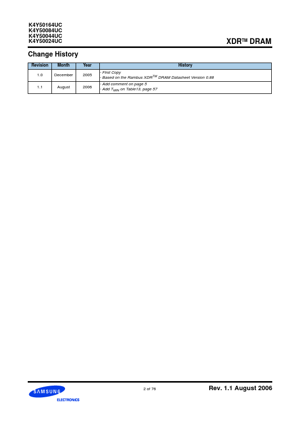
K4Y50024UC Description
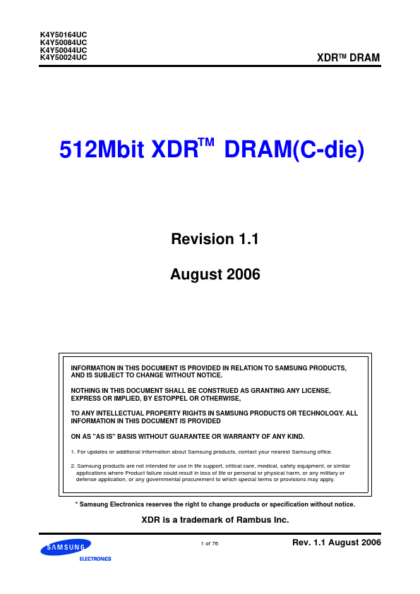
NOTHING IN THIS DOCUMENT SHALL BE CONSTRUED AS GRANTING ANY LICENSE, EXPRESS OR IMPLIED, BY ESTOPPEL OR OTHERWISE, TO ANY INTELLECTUAL PROPERTY RIGHTS IN SAMSUNG PRODUCTS OR TECHNOLOGY. ALL INFORMATION IN THIS DOCUMENT IS PROVIDED ON AS "AS IS" BASIS WITHOUT GUARANTEE OR WARRANTY OF ANY KIND. For updates or additional information about Samsung products, contact your nearest Samsung office.
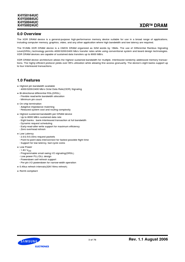
K4Y50024UC Key Features
- Highest pin bandwidth available
- 4000/3200/2400 Mb/s Octal Data Rate(ODR) Signaling
- Bi-directional differential RSL(DRSL)
- Flexible read/write bandwidth allocation
- Minimum pin count
- On-chip termination
- Adaptive impedance matching
- Reduced system cost and routing plexity
- Highest sustained bandwidth per DRAM device
- Up to 8000 MB/s sustained data rate
K4Y50024UC Applications
- Samsung Electronics reserves the right to change products or specification without notice


