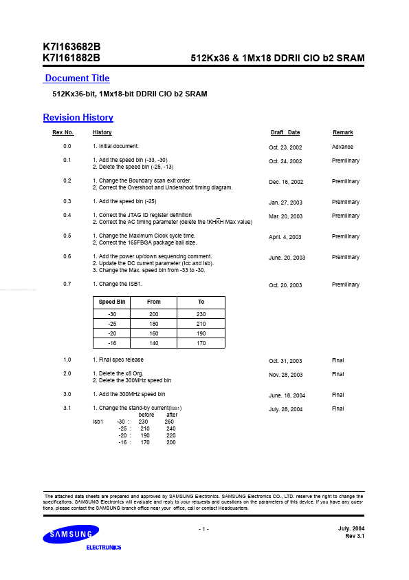
K7I163682B
K7I163682B is 1Mx18-bit DDRII CIO b2 SRAM manufactured by Samsung Semiconductor.
FEATURES
- 1.8V+0.1V/-0.1V Power Supply.
- DLL circuitry for wide output data valid window and future freguency scaling.
- I/O Supply Voltage 1.5V+0.1V/-0.1V for 1.5V I/O, 1.8V+0.1V/-0.1V for 1.8V I/O.
- Pipelined, double-data rate operation.
- mon data input/output bus .
- HSTL I/O
- Full data coherency, providing most current data.
- Synchronous pipeline read with self timed late write.
- Registered address, control and data input/output.
- DDR(Double Data Rate) Interface on read and write ports.
- Fixed 2-bit burst for both read and write operation.
- Clock-stop supports to reduce current.
- Two input clocks(K and K) for accurate DDR timing at clock rising edges only.
- Two input clocks for output data(C and C) to minimize clock-skew and flight-time mismatches.
- Two echo clocks (CQ and CQ) to enhance output data traceability.
- Single address bus.
- Byte write (x18, x36) function.
- Simple depth expansion with no data contention.
- Programmable output impedance.
- JTAG 1149.1 patible test access port.
- 165FBGA(11x15 ball array FBGA) with body size of 13x15mm Organization Part Number...