K7I323682M
K7I323682M is 1Mx36 & 2Mx18 DDRII CIO b2 SRAM manufactured by Samsung Semiconductor.
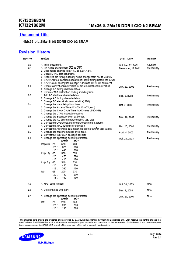
description on page 2 and add HSTL I/O ment 1. Update current characteristics in DC electrical characteristics 2. Change AC timing characteristics 3. Update JTAG instruction coding and diagrams 1. Add AC electrical characteristics. 2. Change AC timing characteristics. 3. Change DC electrical characteristics(ISB1) 1. Change the data Setup/Hold time. 2. Change the Access Time.(t CHQV, t CHQX, etc.) 3. Change the Clock Cycle Time.(MAX value of t KHKH) 4. Change the JTAG instruction coding. 1. Change the Boundary scan exit order. 2. Change the AC timing characteristics(-25, -20) 3. Correct the Overshoot and Undershoot timing diagrams. 1. Correct the JTAG ID register definition 2. Correct the AC timing parameter (delete the t KHKH Max value) 1. Change the Maximum Clock cycle time. 2. Correct the 165FBGA package ball size. 1. Change the operating current parameter. before after Icc(x36) -25 : 620 700 -20 : 520 600 -16 : 440 500 Icc(x18) -25 : 560 670 -20 : 470 570 -16 : 410 470 Icc(x 8 ) -25 : 540 650 -20 : 450 550 -16 : 390 450 Isb1 -25 : 200 230 -20 : 180 200 -16 : 160 190 1. Final spec release 1. Delete the x8 Org. part 1. Change the operating current parameter before after Isb1 -25 : 230 250 -20 : 200 230 -16 : 190 220 Draft Date October, 22 2001 December, 12 2001 Remark Advance Preliminary
July, 29. 2002
Preliminary
Sep. 6. 2002
Preliminary
Oct. 7. 2002
Preliminary
Dec. 16, 2002
Preliminary
0.6 0.7 0.8
Mar. 20, 2003 April. 4, 2003 Oct. 29, 2003
Preliminary Preliminary Preliminary
1.0 2.0 2.1
Oct. 31, 2003 Dec. 1, 2003 July. 27, 2004
Final Final Final
The attached data sheets are prepared and approved by SAMSUNG Electronics. SAMSUNG Electronics CO., LTD. reserve the right to change the specifications. SAMSUNG Electronics will evaluate and reply to your requests and questions on the parameters of this device. If you have any questions, please contact the SAMSUNG branch office near your office, call or contact Headquarters.
-1-
July....