K7I321882M
K7I321882M is 1Mx36 & 2Mx18 DDRII CIO b2 SRAM manufactured by Samsung Semiconductor.
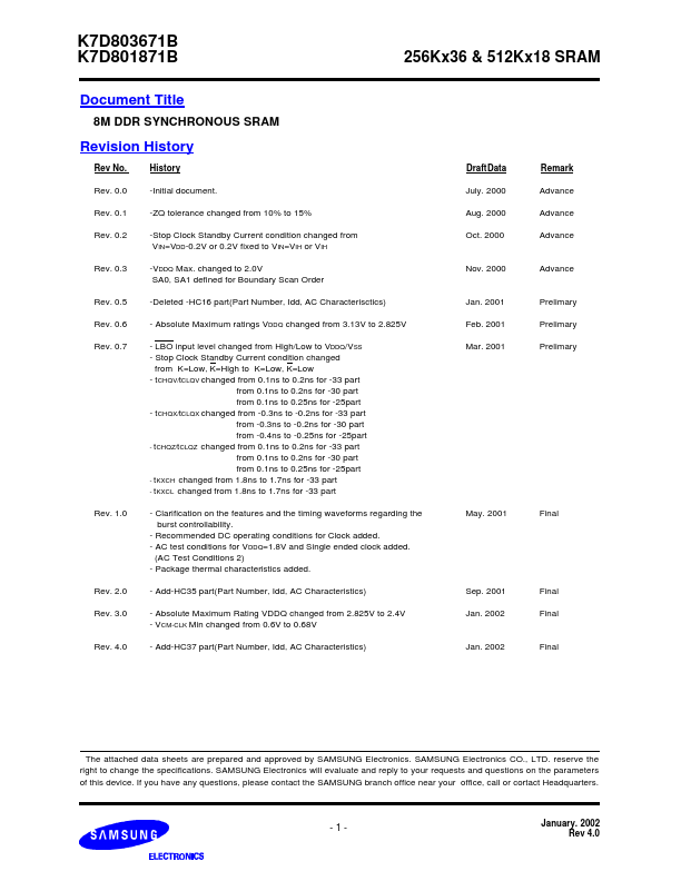
features and the timing waveforms regarding the burst controllability.
- Remended DC operating conditions for Clock added.
- AC test conditions for V DDQ=1.8V and Single ended clock added. (AC Test Conditions 2)
- Package thermal characteristics added.
- Add-HC35 part(Part Number, Idd, AC Characteristics)
- Absolute Maximum Rating VDDQ changed from 2.825V to 2.4V
- V CM-CLK Min changed from 0.6V to 0.68V
- Add-HC37 part(Part Number, Idd, AC Characteristics) Draft Data July. 2000 Aug. 2000 Oct. 2000 Remark Advance Advance Advance
Rev. 0.3
Nov. 2000
Advance
Rev. 0.5 Rev. 0.6 Rev. 0.7
Jan. 2001 Feb. 2001 Mar. 2001
Prelimary Prelimary Prelimary
Rev. 1.0
May. 2001
Final
Rev. 2.0 Rev. 3.0
Sep. 2001 Jan. 2002
Final Final
Rev. 4.0
Jan. 2002
Final
The attached data sheets are prepared and approved by SAMSUNG Electronics. SAMSUNG Electronics CO., LTD. reserve the right to change the specifications. SAMSUNG Electronics will evaluate and reply to your requests and questions on the parameters of this device. If you have any questions, please contact the SAMSUNG branch office near your office, call or cortact Headquarters.
-1-
January. 2002 Rev 4.0
K7D803671B K7D801871B
FEATURES
- -
- -
- -
- -
- -
- -
- -
- -
- 256Kx36 & 512Kx18 SRAM
Maximum Frequency 370MHz 357MHz 333MHz 300MHz 250MHz 370MHz 357MHz 333MHz 300MHz 250MHz Access Time 1.7- 1.7- 1.7- 1.9- 2.0- 1.7- 1.7- 1.7- 1.9- 2.0-
Organization Part Number 256Kx36 or 512Kx18 Organizations. Maximum Frequency : 370MHz (Data Rate : 740Mbps) 2.5V V DD/1.5V VDDQ (2.0V max VDDQ). K7D803671B-HC37 HSTL Input and Outputs. K7D803671B-HC35 Single Differential HSTL Clock. 256Kx36 K7D803671B-HC33 Synchronous Pipeline Mode of Operation with Self-Timed Late Write. Free Running Active High and Active Low Echo Clock Output Pin. K7D803671B-HC30 Asynchronous Output Enable. K7D803671B-HC25 Registered...