K7P161866A
K7P161866A is 512Kx36 AND 1Mx18 Synchronous Pipelined SRAM manufactured by Samsung Semiconductor.
..
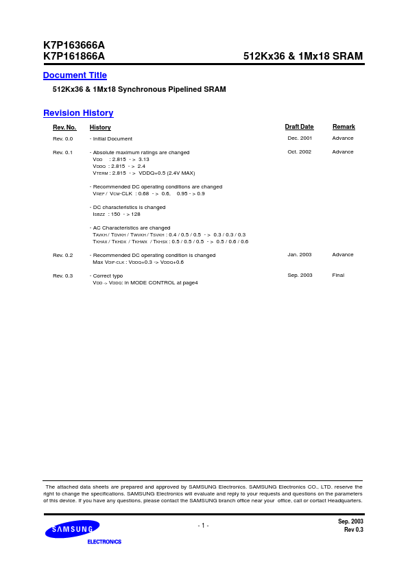
K7P163666A K7P161866A
Document Title
512Kx36 & 1Mx18 Synchronous Pipelined SRAM
512Kx36 & 1Mx18 SRAM
Revision History
Rev. No.
Rev. 0.0 Rev. 0.1
History
- Initial Document
-...