K7P403623B
K7P403623B is 128Kx36 & 256Kx18 SRAM manufactured by Samsung Semiconductor.
K7P403623B K7P401823B
Document Title
128Kx36 & 256Kx18 Synchronous Pipelined SRAM
128Kx36 & 256Kx18 SRAM
Revision History
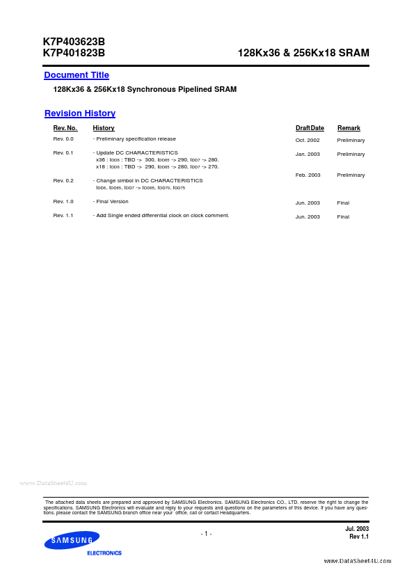
Rev. No.
Rev. 0.0 Rev. 0.1
History
- Preliminary specification release
- Update DC CHARACTERISTICS x36 : IDD6 : TBD -> 300, IDD65 -> 290, IDD7 -> 280. x18 : IDD6 : TBD -> 290, IDD65 -> 280, IDD7 -> 270.
- Change simbol in DC CHARACTERISTICS IDD6, IDD65, IDD7 -> IDD65, IDD70, IDD75
- Final Version
- Add Single ended differential clock on clock ment.
Draft Date
Oct. 2002 Jan. 2003
Remark
Preliminary Preliminary
Feb. 2003 Rev. 0.2
Preliminary
Rev. 1.0 Rev. 1.1
Jun. 2003 Jun. 2003
Final Final
..
The attached data sheets are prepared and...