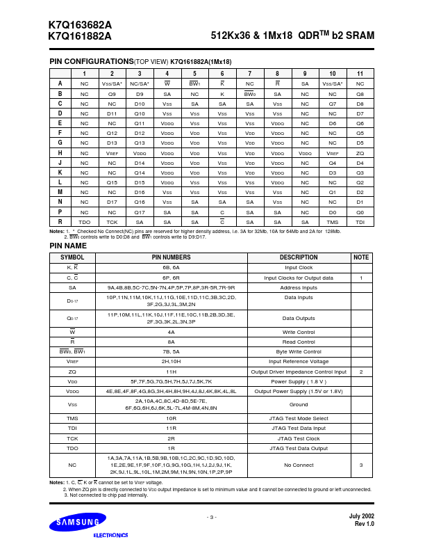
Datasheet4U Logo Datasheet4U.com

K7Q161882A - (K7Q161882A / K7Q161882A) 512Kx36 & 1Mx18 QDR b2 SRAM

General Description

Input Clock Input Clocks for Output data Address Inputs Data Inputs 1 NOTE Data Outputs Write Control Read Control Byte Write Control Input Reference Voltage Output Driver Impedance Control Input Power Supply ( 1.8 V ) Output Power Supply (1.5V or 1.8V) Ground JTAG Test Mode Select JTAG Test Data I

Key Features

  • 1.8V+0.1V/-0.1V Power Supply.
  • I/O Supply Voltage 1.5V+0.1V/-0.1V for 1.5V I/O, 1.8V+0.1V/-0.1V for 1.8V I/O.
  • Separate independent read and write data ports with concurrent read and write operation.
  • HSTL I/O.
  • Full data coherency, providing most current data.
  • Synchronous pipeline read with self timed early write.
  • Registered address, control and data input/output.
  • DDR(Double Data Rate) Interface on read and write ports.

📥 Download Datasheet

Full PDF Text Transcription (Reference)

The following content is an automatically extracted verbatim text from the original manufacturer datasheet and is provided for reference purposes only.

View original datasheet text
www.DataSheet4U.com K7Q163682A K7Q161882A Document Title 512Kx36-bit, 1Mx18-bit QDRTM SRAM 512Kx36 & 1Mx18 QDRTM b2 SRAM Revision History Rev. No. 0.0 0.1 History 1. Initial document. 1. Icc, Isb addition 2. 1.8V Vddq addition 3. Speed bin change 1. Changed Pin configuration at x36 organization. - 9F ; from Q14 to D14 . - 10F ; from D14 to Q14 . 2. Reserved pin for high density name change from NC to Vss/SA 1. Final SPEC release 2. Modify thermal resistance Draft Date May, 22 2001 Remark Advance Sep,03 2001 Advance 0.2 Nov.
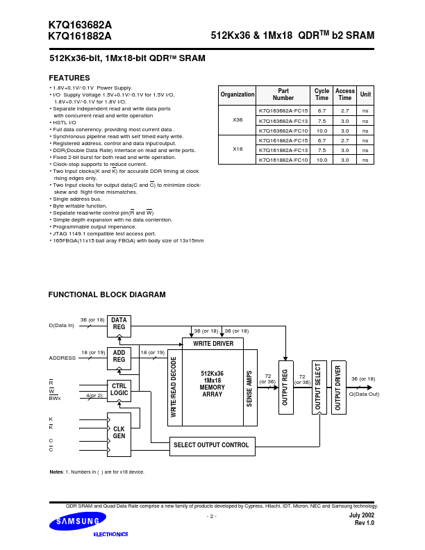
 20. 2001 Preliminary 1.0 July, 03. 2002 Final The attached data sheets are prepared and approved by SAMSUNG Electronics. SAMSUNG Electronics CO., LTD. reserve the right to change the specifications.