Datasheet4U Logo Datasheet4U.com

K7Q163652A - (K7Q161852A / K7Q163652A) 512Kx36 & 1Mx18 QDRTM b2 SRAM

Download the K7Q163652A datasheet PDF. This datasheet also covers the K7Q161852A variant, as both devices belong to the same (k7q161852a / k7q163652a) 512kx36 & 1mx18 qdrtm b2 sram family and are provided as variant models within a single manufacturer datasheet.

General Description

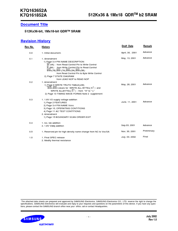
W (4A) : from Read Control Pin to Write Control R (8A) : from Write Control Pin to Read Control BW0(7B),BW1(7A),BW2(5A),BW3(5B) : from Read Control Pin to Byte Wrtie Control 2) Page 7 STATE DIAGRAM from LEAD NOP to READ NOP 1.

Key Features

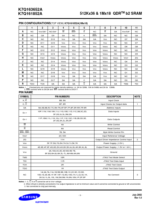
  • 2) Page 3,4 PIN NAME VDDQ 3) Page 10,.

📥 Download Datasheet

Note: The manufacturer provides a single datasheet file (K7Q161852A_Samsungsemiconductor.pdf) that lists specifications for multiple related part numbers.

Full PDF Text Transcription (Reference)

The following content is an automatically extracted verbatim text from the original manufacturer datasheet and is provided for reference purposes only.

View original datasheet text
www.DataSheet4U.com K7Q163652A K7Q161852A Document Title 512Kx36-bit, 1Mx18-bit QDRTM SRAM 512Kx36 & 1Mx18 QDRTM b2 SRAM Revision History Rev. No. 0.0 0.1 History 1. Initial document. 1. Amendment 1) Page 3,4 PIN NAME DESCRIPTION W (4A) : from Read Control Pin to Write Control R (8A) : from Write Control Pin to Read Control BW0(7B),BW1(7A),BW2(5A),BW3(5B) : from Read Control Pin to Byte Wrtie Control 2) Page 7 STATE DIAGRAM from LEAD NOP to READ NOP 1. Amendment 1) Page 8 WRITE TRUTH TABLE(x36) BW2,BW3 values for WRITE ALL BYTEs( K↑ ) and WRITE ALLBYTEs( K↑ ) : from "H" to " L" 2) Page 13 TIMING WAVE FORMS Note 2 supplement 1. 1.8V I/O supply voltage addition 1) Page 2 FEATURES 2) Page 3,4 PIN NAME VDDQ 3) Page 10, OPERATING CONTITIONS 4) Page 11 AC TEST CONTITIONS 2.