K7Q163654A Description
from Read Control Pin to Write Control R (8A) : from Write Control Pin to Read Control BW0(7B),BW1(7A),BW2(5A),BW3(5B) : from Read Control Pin to Byte Wrtie Control 2) Page 7 STATE DIAGRAM from LEAD NOP to READ NOP.
K7Q163654A Key Features
- 2.5V+0.1V/-0.1V Power Supply
- I/O Supply Voltage 1.5V+0.1V/-0.1V for 1.5V I/O, 1.8V+0.1V/-0.1V for 1.8V I/O
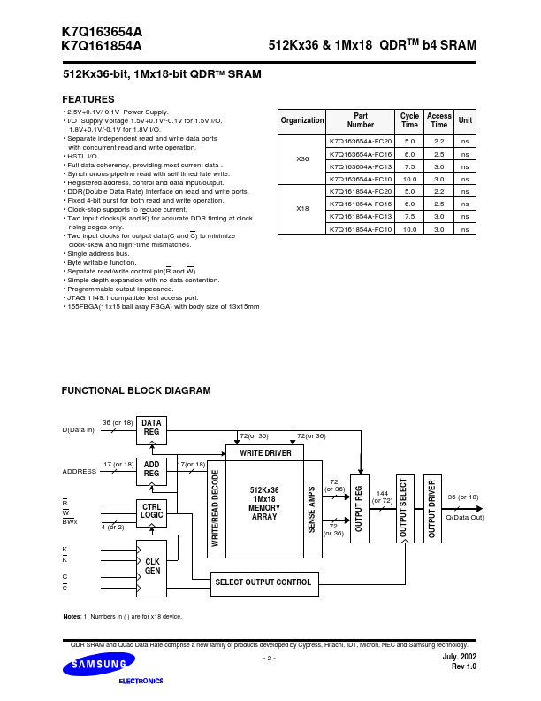
- Separate independent read and write data ports with concurrent read and write operation
- HSTL I/O
- Full data coherency, providing most current data
- Synchronous pipeline read with self timed late write
- Registered address, control and data input/output
- DDR(Double Data Rate) Interface on read and write ports
- Fixed 4-bit burst for both read and write operation
- Clock-stop supports to reduce current