KM718V887
KM718V887 is 256Kx18 Synchronous SRAM manufactured by Samsung Semiconductor.
Document Title
256Kx18-Bit Synchronous Burst SRAM
256Kx18 Synchronous SRAM
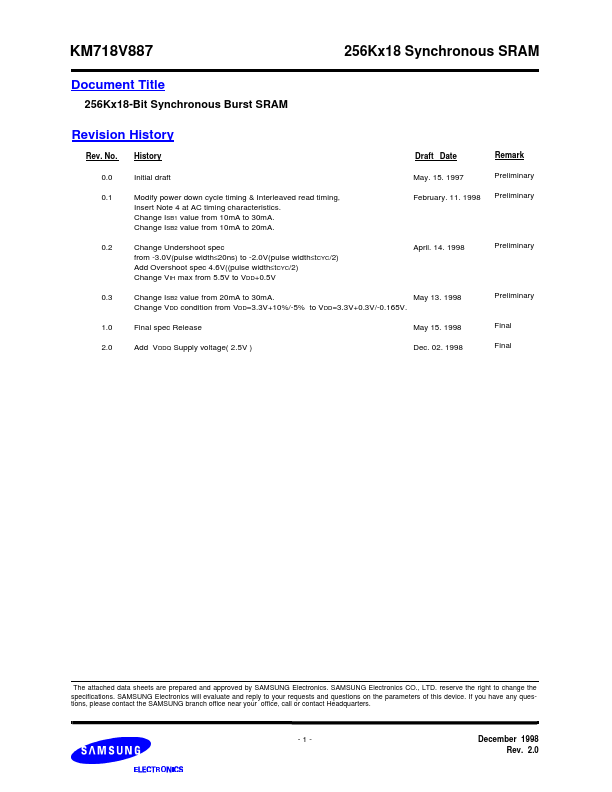
Revision History
Rev. No. 0.0 0.1 History Initial draft Modify power down cycle timing & Interleaved read timing, Insert Note 4 at AC timing characteristics. Change ISB1 value from 10mA to 30mA. Change ISB2 value from 10mA to 20mA. Change Undershoot spec from -3.0V(pulse width≤20ns) to -2.0V(pulse width≤tCYC/2) Add Overshoot spec 4.6V((pulse width≤tCYC/2) Change VIH max from 5.5V to VDD+0.5V Draft Date May. 15. 1997 February. 11. 1998 Remark Preliminary Preliminary
April. 14. 1998
Preliminary
May 13. 1998 Change ISB2 value from 20mA to 30mA. Change VDD condition from VDD=3.3V+10%/-5% to...