Datasheet Summary
128MB, 256MB SODIMM Pb-Free
DDR SDRAM
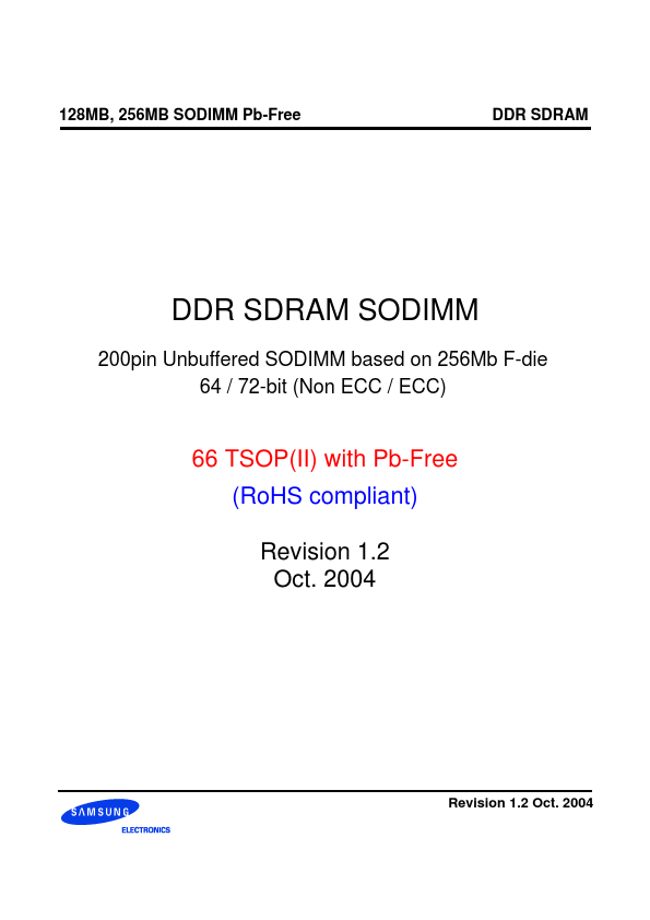
DDR SDRAM SODIMM
200pin Unbuffered SODIMM based on 256Mb F-die 64 / 72-bit (Non ECC / ECC)
66 TSOP(II) with Pb-Free (RoHS pliant) Revision 1.2 Oct. 2004
Revision 1.2 Oct. 2004
128MB, 256MB SODIMM Pb-Free
Revision History
Revision 1.0 (February, 2004)
- First release Revision 1.1 (March, 2004)
- Corrected package dimension. Revision 1.2 (Oct, 2004)
- Corrected typo.
DDR SDRAM
Revision 1.2 Oct. 2004
128MB, 256MB SODIMM Pb-Free
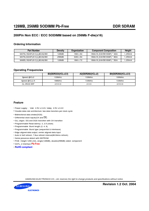
200Pin Non ECC / ECC SODIMM based on 256Mb F-die(x16)
Ordering Information
Part Number M470L1624FU0-C(L)B3/A2/B0 M470L3224FU0-C(L)B3/A2/B0 M485L1624FU0-C(L)B3/A2/B0 Density 128MB 256MB 128MB Organization 16M x 64 32M x...