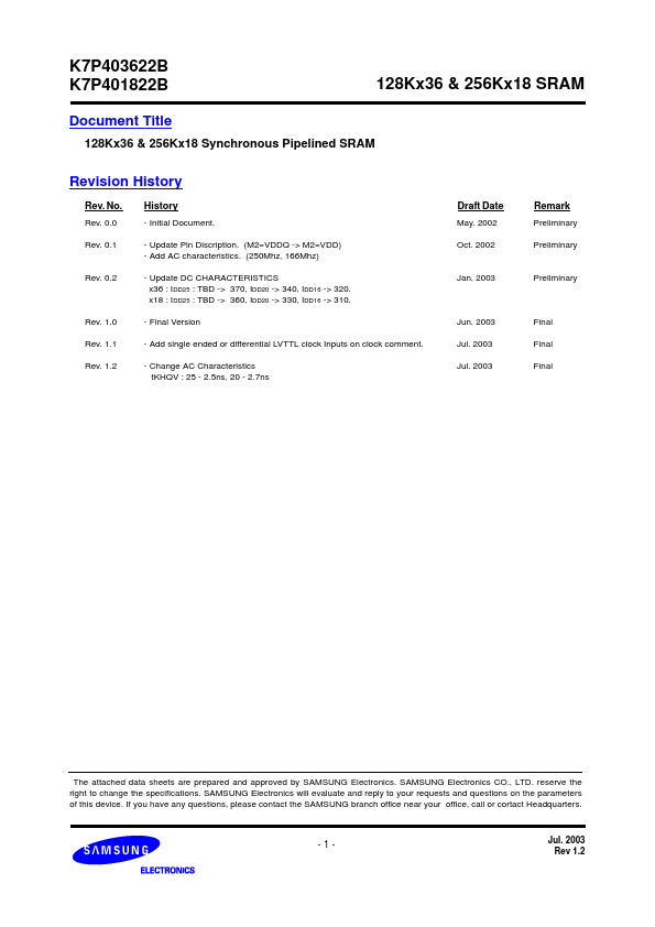
K7P401822B
K7P401822B is SRAM manufactured by Samsung Semiconductor.
- Part of the K7P403622B comparator family.
- Part of the K7P403622B comparator family.
FEATURES
- 128Kx36 or 256Kx18 Organizations.
- 3.3V VDD, 2.5/3.3V VDDQ.
- LVTTL Input and Output Levels.
- Differential, PECL clock / Single ended or differential LVTTL clock Inputs
- Synchronous Read and Write Operation.
- Registered Input and Registered Output.
- Internal Pipeline Latches to Support Late Write.
- Byte Write Capability(four byte write selects, one for each 9bits)
- Synchronous or Asynchronous Output Enable.
- Power Down Mode via ZZ Signal.
- JTAG Boundary Scan (subset of IEEE std. 1149.1).
- 119(7x17)Pin Ball Grid Array Package(14mmx22mm).
Organization
Part Number
128Kx36 128Kx36 128Kx36 256Kx18 256Kx18 256Kx18
K7P403622B-HC25 K7P403622B-HC20 K7P403622B-HC16 K7P401822B-HC25 K7P401822B-HC20 K7P401822B-HC16
Maximum Access Frequency Time
250MHz
200MHz
166MHz
250MHz
200MHz
166MHz
FUNCTIONAL BLOCK DIAGRAM
SA[0:16] or [0:17]
K,K
Clock Buffer
Read Address Register
17 or 18
Write Address
Register
17 or 18
2:1...