BF543 Overview
Key Specifications
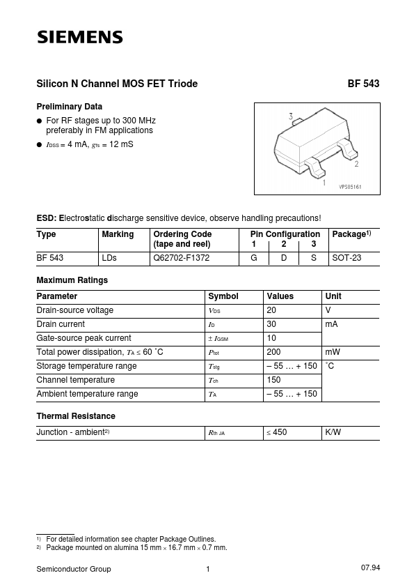
Package: SOT-23
Mount Type: Surface Mount
Pins: 3
Height: 1.12 mm
Key Features
- ambient2) Rth JA
- 55 … + 150 ˚C
| Part | BF543 |
|---|---|
| Description | Silicon N Channel MOS FET Triode |
| Manufacturer | Siemens Semiconductor Group |
| Size | 97.31 KB |
Package: SOT-23
Mount Type: Surface Mount
Pins: 3
Height: 1.12 mm
| Seller | Inventory | Price Breaks | Buy |
|---|---|---|---|
| Farnell | 0 | 5+ : 0.36 GBP 25+ : 0.34 GBP 100+ : 0.194 GBP 250+ : 0.171 GBP |
View Offer |
| Farnell | 0 | 100+ : 0.194 GBP 250+ : 0.171 GBP 500+ : 0.15 GBP 1000+ : 0.128 GBP |
View Offer |
| Part Number | Manufacturer | Description |
|---|---|---|
| BF543 | Infineon | Silicon N-Channel MOSFET Triode |
| BF545C | NXP Semiconductors | N-channel silicon junction field-effect transistors |
| BF545A | NXP Semiconductors | N-channel silicon junction field-effect transistors |
| BF547 | NXP Semiconductors | NPN 1 GHz wideband transistor |
| ADSP-BF542 | Analog Devices | Embedded Processor |