SI53115 Overview
Key Specifications
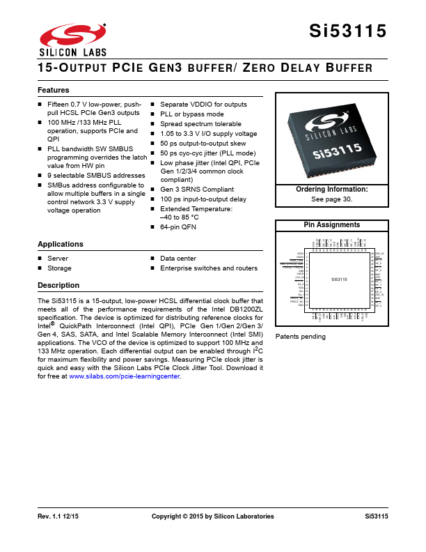
Package: QFN
Mount Type: Surface Mount
Pins: 64
Operating Voltage: 3.3 V
Description
The Si53115 is a 15-output, low-power HCSL differential clock buffer that meets all of the performance requirements of the Intel DB1200ZL specification. The device is optimized for distributing reference clocks for Intel® QuickPath Interconnect (Intel QPI), PCIe Gen 1/Gen 2/Gen 3/ Gen 4, SAS, SATA, and Intel Scalable Memory Interconnect (Intel SMI) applications.
Key Features
- Fifteen 0.7 V low-power, push
- Separate VDDIO for outputs pull HCSL PCIe Gen3 outputs
- PLL or bypass mode
- 100 MHz /133 MHz PLL
- Spread spectrum tolerable